How to Choose a Pull-Up Resistor Value (With I2C Math)

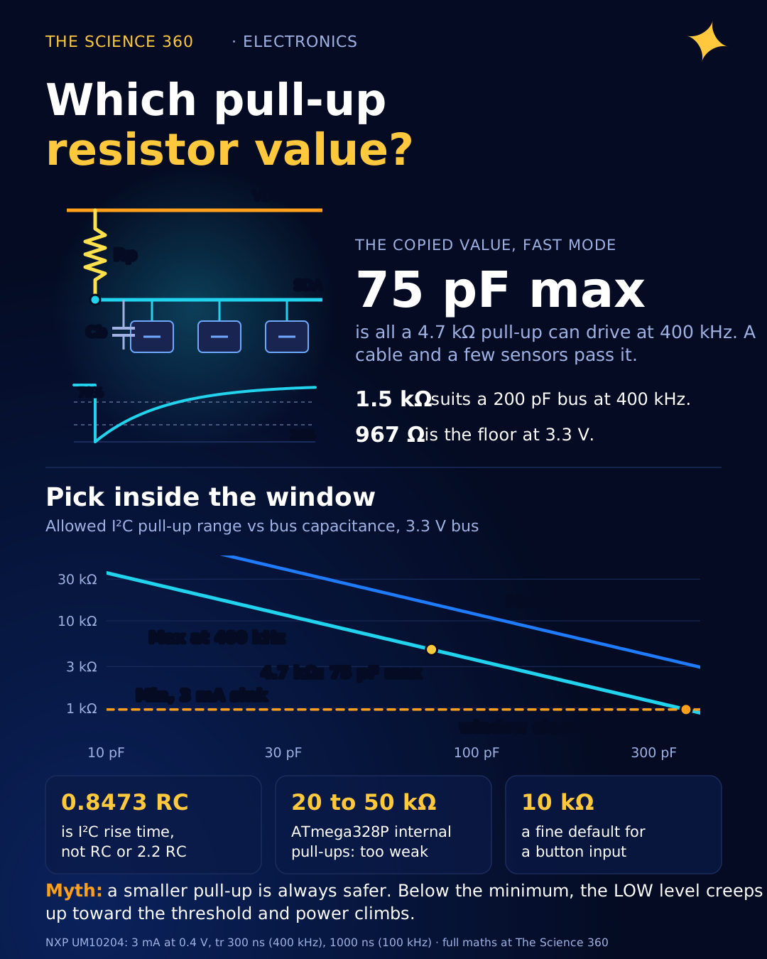
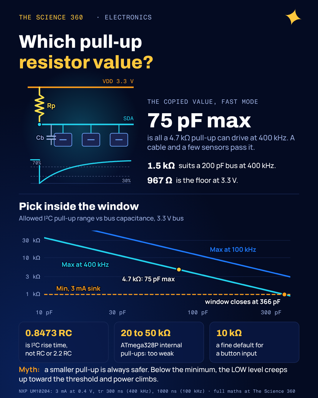
4.7 kΩ is probably the most copied number in hobby electronics. It is on breakout boards, in tutorials and in half the I²C schematics on the internet. Run the arithmetic from the I²C specification and you find that at 400 kHz, a 4.7 kΩ pull-up meets the rise-time limit only while the bus capacitance stays below 75 pF. Add a 30 cm ribbon cable and a few sensors and you are past it. The bus usually keeps working anyway, which is exactly why the number survives.
This post shows where pull-up values actually come from: a lower bound, an upper bound, and a calculation that tells you which side of the window you are on. The same reasoning covers buttons and plain GPIO inputs, where the numbers are far more forgiving.
What does a pull-up resistor actually do?
A pull-up gives a line a defined HIGH level when nothing is actively driving it. That matters in two situations. An input pin connected to a button floats when the button is open, and a floating CMOS input drifts with stray fields. And open-drain buses such as I²C are built so that every device can only pull the line LOW; nobody drives it HIGH. The resistor is the only thing that brings it back up.
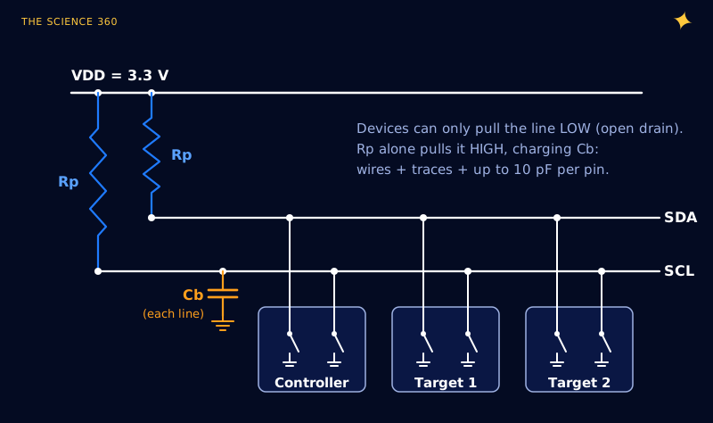
That second job is why pull-up value matters on buses. Pulling the line low is fast, because a transistor does it with tens of milliamps of drive. Letting it go high is slow, because the only current available is what flows through Rp. The rising edge is an RC charging curve, and the time constant is set by your resistor.
Why is there a minimum pull-up value?
When a device pulls the line low, it has to sink the current flowing down through the pull-up. If Rp is too small, that current exceeds what the output transistor can sink while staying near 0 V, and the LOW level climbs. NXP's I²C specification (UM10204) guarantees that Standard-mode and Fast-mode outputs can sink 3 mA with VOL no higher than 0.4 V. Fast-mode Plus parts are guaranteed 20 mA.
Minimum pull-up, Standard and Fast mode
5.5 V is the worst case (5 V + 10%) and the spec's own example.
Go below this and nothing explodes. What happens is quieter: the LOW level might sit at 0.6 or 0.8 V instead of 0.4 V, eating into the 0.3 VDD threshold (0.99 V at 3.3 V) that receivers use to recognize a zero. Add ground bounce and a weak driver at high temperature and you get the occasional corrupted byte that nobody can reproduce on the bench.
Why is there a maximum pull-up value?
There are two upper limits, and on I²C the first one almost always wins.
The rise-time limit, and where 0.8473 comes from
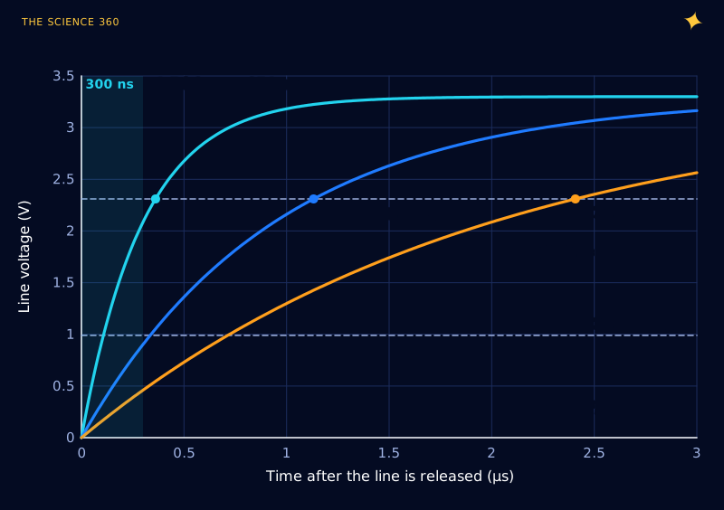
When the line is released, it charges as . I²C defines rise time between the 30% and 70% levels, because those are the input thresholds VIL and VIH. Solve for each crossing:
So:
tr(max) is 1000 ns for Standard-mode (100 kHz), 300 ns for Fast-mode (400 kHz) and 120 ns for Fast-mode Plus (1 MHz).
A common misconception is that rise time "is" RC, or the 10% to 90% time of 2.2 RC that you learn for oscilloscopes. Use either for I²C and you will be wrong by a factor of 1.2 or 2.6. The 0.8473 factor is in UM10204 itself, derived exactly as above.
The leakage limit
Every input on the bus leaks a little current, up to 10 µA per pin in the I²C specification. That current flows through Rp and drags the HIGH level down. UM10204 asks for a HIGH-level noise margin of 0.2 VDD:
3.3 V bus with 5 devices:
This bound is real but rarely the one that bites, since the rise-time limit is usually much lower. It matters on slow buses with many devices, and on general-purpose inputs where rise time does not matter at all.
Worked example: 3.3 V I²C at 400 kHz with a 200 pF bus
Say you have a controller, four sensors and a 40 cm cable to a second board. You measured or estimated 200 pF of total capacitance on each line (more on estimating below).
Step 1. Lower bound (sink current)
Step 2. Upper bound (rise time)
Step 3. Upper bound (leakage, 6 pins)
Not limiting.
Step 4. Pick a standard value inside 967 Ω to 1,770 Ω
1.5 kΩ (E12) gives a 15% margin on rise time, a sink current inside 3 mA, and this supply current while a line is LOW:
The window is narrow: less than a factor of two. Figure 3 shows why. As the bus capacitance grows, the maximum falls until it crosses the minimum, and past that point no resistor will do.
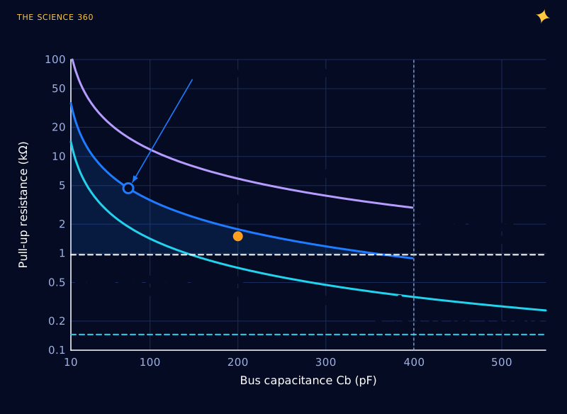
That closing point is worth a second look. Plug Rmin = 967 Ω into the rise-time equation and you get . On a 3.3 V bus with plain 3 mA devices, you cannot actually use the full 400 pF that Fast mode permits. The spec itself flags this: its footnote says full bus load at 400 kHz needs 6 mA of sink current at VOL = 0.6 V. For bigger buses, the fixes are Fast-mode Plus drivers, a bus buffer that splits the capacitance, or a switched (active) pull-up circuit, all described in UM10204.
Is a smaller pull-up always safer?
This is the second misconception, and it comes from people who were burned by slow edges. Lower resistance does give faster edges and better noise immunity. But below Rmin you trade a visible problem (slow edges) for an invisible one (LOW levels creeping toward the threshold), and you pay in power the whole time. On a battery sensor that holds SDA low for half of every transfer, 1 kΩ at 3.3 V costs 3.3 mA per line while low, while 4.7 kΩ costs 0.7 mA. NXP's own advice is that portable designs should sit toward the high end of the window to save supply current. The goal is to land inside the window, not at one wall of it.
How do you estimate bus capacitance?
You need Cb for the calculation, and it is the number most people skip. Two practical approaches:
- Add it up. The I²C specification allows each device pin up to 10 pF. Add the PCB traces (a typical trace over a ground plane is on the order of 1 pF per centimetre, depending on geometry) and any cable, which typically adds something like 50 to 100 pF per metre. Then add 20 to 30% margin for things you forgot, like a logic analyser probe.
- Measure it. This is the better option and takes two minutes. Fit any pull-up, put a scope on SDA, and time the edge from 30% to 70% of VDD. Then Cb = tr / (0.8473 Rp). With a 4.7 kΩ pull-up and a measured 400 ns rise time, Cb = 400 ns / (0.8473 × 4,700) = 100 pF. Use a 10x probe; a 1x probe adds its own 50 pF or more.
When are internal MCU pull-ups too weak?
Most microcontrollers have pull-ups you can enable in software, and they are deliberately weak to save current. The ATmega328P (Arduino Uno) specifies 20 to 50 kΩ. The RP2040 (Raspberry Pi Pico) specifies 50 to 80 kΩ. Figure 4 shows what those values mean for I²C.
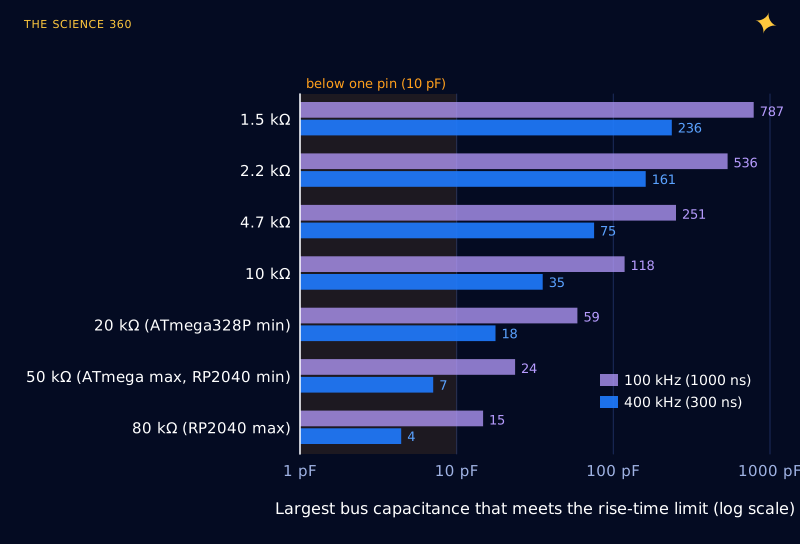
So internal pull-ups are the wrong tool for I²C, with one honest exception: very short, slow buses where the rise time violates the spec but the receiver still sees a clean level before the clock samples it. That "works on my desk" case is where most of the folklore about internal pull-ups comes from. It is not a design, it is a coincidence.
Where internal pull-ups are perfectly good: buttons, jumpers, DIP switches and other inputs that change at human speed and sit right next to the chip.
Pull-ups for buttons and plain GPIO inputs
Without a rise-time deadline, the window for a button is enormous. The bounds become:
Upper bound: leakage (ATmega328P at 5 V)
Input leakage IIH is at most 1 µA, and the pin is guaranteed HIGH above :
Lower bound: current while pressed
3.3 mA is wasteful for a button held down.
Nobody should use 2 MΩ, though. A high-impedance node acts as an antenna, and dust, flux residue and humidity on the board can leak far more than the chip's 1 µA. The practical range is roughly 4.7 kΩ to 47 kΩ, and 10 kΩ is a fine default. Go stronger (1 to 4.7 kΩ) when the button sits at the end of a long cable in an electrically noisy box, because a lower impedance makes induced noise currents produce smaller voltages. Pair it with a small capacitor for debouncing and EMI filtering if needed.
FAQ
What value pull-up resistor should I use for I2C?
Compute a window. The minimum is (VDD minus 0.4 V) divided by 3 mA, about 970 Ω at 3.3 V. The maximum is the rise-time limit divided by 0.8473 times the bus capacitance: 300 ns for 400 kHz, 1000 ns for 100 kHz. For a 200 pF bus at 400 kHz that gives 1.77 kΩ, so 1.5 kΩ is a good choice.
Is 10k too high for an I2C pull-up?
Usually, yes. A 10 kΩ pull-up meets the 400 kHz rise-time limit only if the total bus capacitance is below about 35 pF, and the 100 kHz limit only below about 118 pF. It can work on a tiny board with one or two devices, but it leaves little margin.
Can I use the microcontroller’s internal pull-ups for I2C?
Rarely. Internal pull-ups are typically 20 to 80 kΩ (20 to 50 on an ATmega328P, 50 to 80 on an RP2040). At 50 kΩ the Standard-mode rise-time limit allows only about 24 pF of bus capacitance, which a couple of chips and a short cable already exceed. Use external resistors.
What happens if a pull-up resistor is too small?
The driver pulling the line low has to sink more current than it is guaranteed to handle, so the LOW voltage rises and may no longer be read as a logic 0. It also wastes power whenever the line is low. For I²C, devices are only guaranteed to sink 3 mA at 0.4 V in Standard and Fast mode.
What pull-up resistor value should I use for a button?
Anything from about 4.7 kΩ to 47 kΩ works for a button next to the microcontroller; 10 kΩ is a sensible default. Speed is irrelevant for a human press, so the choice trades current while pressed (330 µA at 3.3 V with 10 kΩ) against noise pickup on long wires.
Related on The Science 360
Sources
- NXP Semiconductors, UM10204 I²C-bus specification and user manual, Rev. 7.0 (2021): Table 10 (VOL, IOL, tr, Cb, Ci, Ii), Section 7.1 pull-up sizing and the 0.8473 RC derivation, Section 7.4 input leakage: nxp.com/docs/en/user-guide/UM10204.pdf
- Texas Instruments, SLVA689 "I2C Bus Pullup Resistor Calculation" (R. Arora, 2015): ti.com/lit/SLVA689
- Microchip (Atmel), ATmega328P automotive datasheet 7810D, Section 28.2 DC characteristics (RPU 20 to 50 kΩ, IIH 1 µA, VIH 0.6 VCC): ww1.microchip.com ATmega328P datasheet PDF
- Raspberry Pi Ltd, RP2040 datasheet, GPIO electrical specifications (pull-up resistance 50 to 80 kΩ): datasheets.raspberrypi.com/rp2040/rp2040-datasheet.pdf
All curves in this post are computed from the equations shown, using the limits in UM10204 Rev. 7.0. PCB trace and cable capacitance figures are typical orders of magnitude; measure your own bus when it matters.
Header image: NASA/ESA (Sophie Adenot) (image iss075e0103086), regraded for this article.