MOSFET Gate Resistor Value: How to Choose It (With Math)

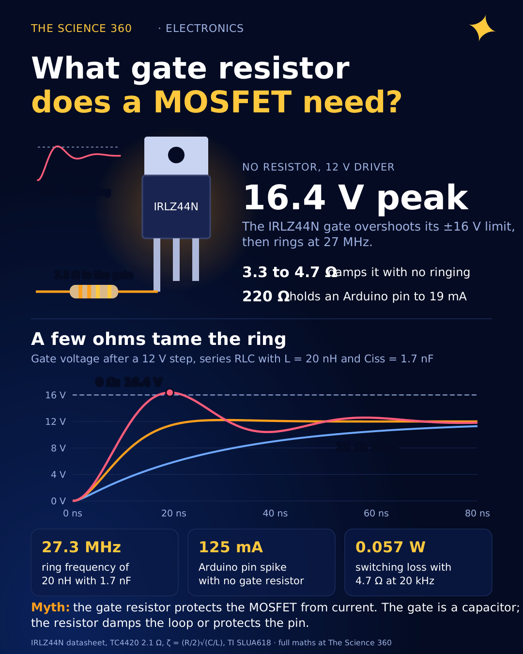
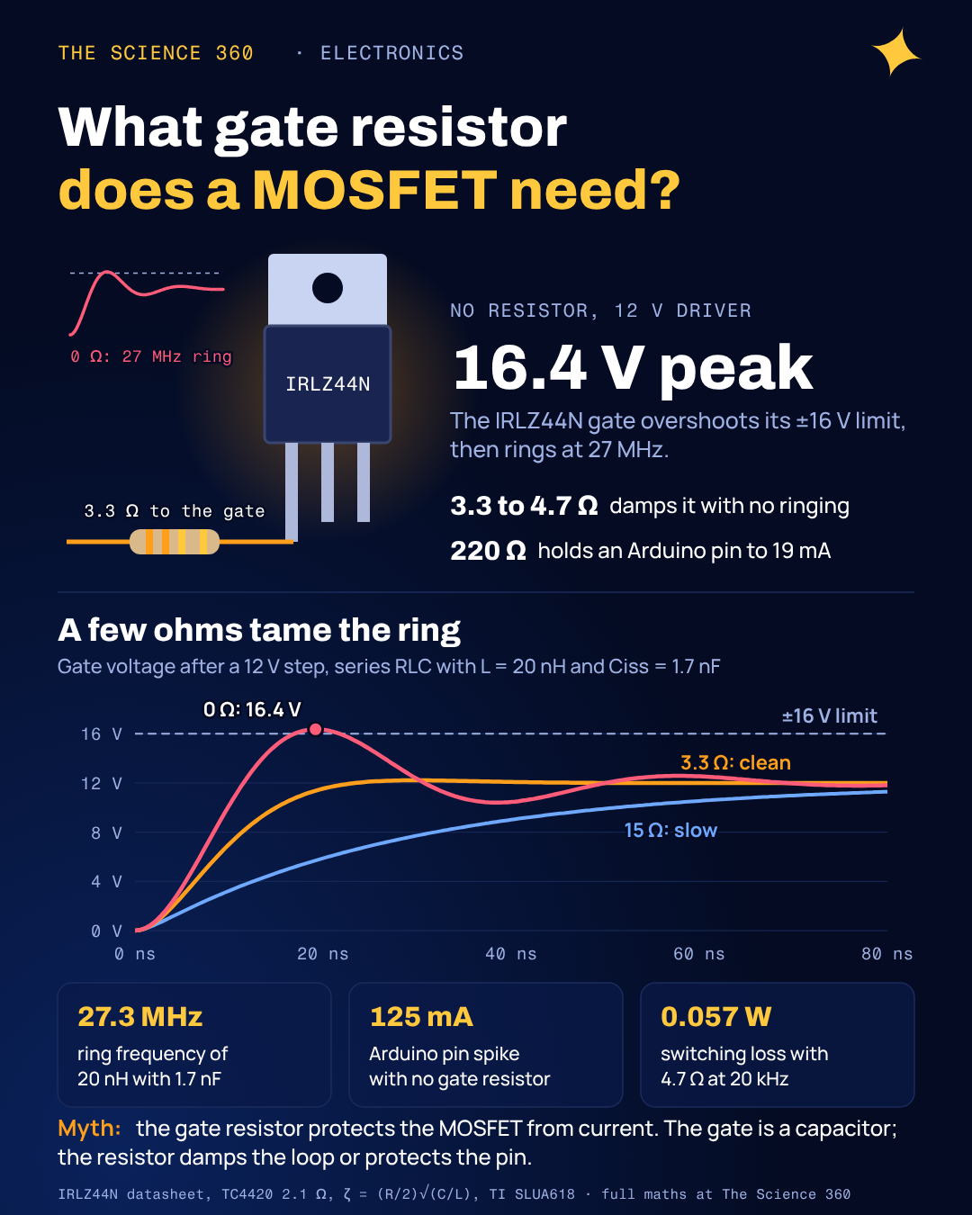
Drive an IRLZ44N from a 12 V gate driver with no gate resistor and a reasonably tidy 2 cm layout, and the gate does not stop at 12 V. In our simulation it overshoots to 16.4 V within 20 ns, then rings at 27 MHz. The part's absolute maximum gate-source voltage is ±16 V. Nothing on the schematic looks wrong. The problem is two components that are not on the schematic at all: the inductance of the gate loop and the capacitance of the gate itself.
Most advice on gate resistors is either a magic number ("use 10 Ω", "use 220 Ω") or a hand wave about "limiting current". Both numbers can be right, for completely different reasons. This post separates the two cases and gives you the calculation for each.
What is a MOSFET gate, electrically?
To the circuit driving it, a MOSFET gate looks like a capacitor. The IRLZ44N datasheet lists an input capacitance Ciss of 1,700 pF and a total gate charge of up to 48 nC. To turn the transistor on you must push that charge in; to turn it off you must pull it out. The faster you want to switch, the larger the current.
That capacitor is not connected by ideal wires. The gate current flows out of the driver, along a trace, through the gate lead and bond wire, across the gate oxide, and back through the source lead and a ground return to the driver. Every millimetre of that loop has inductance. The IRLZ44N datasheet quotes 7.5 nH of internal source inductance alone. PCB rules of thumb put a trace at roughly 0.5 to 1 nH per millimetre, depending on how close its return path runs. A total gate loop of 10 to 40 nH is normal for a through-hole part on a small board.
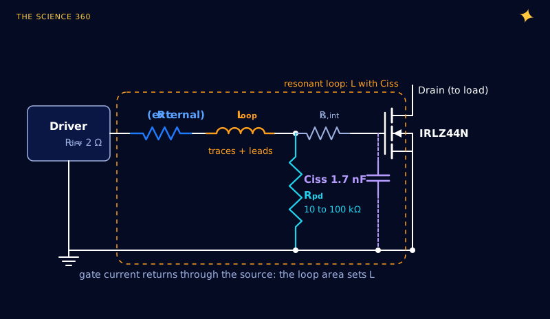
A resistor, an inductor and a capacitor in series: that is the textbook RLC circuit, and the gate resistor is the only part of it you get to choose freely.
The misconception: “the gate resistor limits current to protect the MOSFET”
You will read that a gate resistor "protects the MOSFET from too much current". The MOSFET's gate does not care how much current flows into it; gate current is just charge arriving at a capacitor. What the resistor actually does depends on what is driving the gate:
- With a gate driver IC (amps of peak current, ohms of output resistance), the gate resistor mainly damps the RLC loop so the gate voltage does not overshoot and ring. It also sets switching speed, which matters for EMI and losses.
- With a microcontroller pin (tens of milliamps, tens of ohms), the loop is already heavily damped by the pin's own resistance. Here the resistor protects the pin, not the MOSFET, by limiting the current spike when the gate charges.
A second, related myth: "more gate resistance is always safer". Past the point of critical damping, extra resistance only slows the edges, and slow edges cost heat in the MOSFET. We will quantify that below.
How do you calculate the gate resistor for damping?
For a series RLC circuit, the damping ratio is:
ζ < 1 is underdamped (overshoot and ringing). ζ = 1 is critically damped, the fastest edge with no overshoot. ζ = 0.7 gives about 4.6% overshoot and is slightly faster than ζ = 1.
Setting ζ = 1 gives Texas Instruments' recommended value from its gate-driver application report SLUA618: . Many designers aim slightly lower, around ζ = 0.7, and accept a few percent of overshoot for faster switching.
Worked example: IRLZ44N with a 12 V gate driver
Numbers: Ciss = 1,700 pF (IRLZ44N datasheet, typical). Loop inductance L = 20 nH, our estimate of 7.5 nH of package source inductance plus about 15 mm of loop path at roughly 0.8 nH/mm. Driver: a Microchip TC4420, with a typical source (high-side) output resistance of 2.1 Ω. The IRLZ44N datasheet does not specify its internal gate resistance, so we leave it out; that errs toward choosing a slightly larger external resistor.
Step 1. Characteristic impedance of the loop
Step 2. Natural frequency (what you would see ringing)
Step 3. Damping with no external resistor
That is above the ±16 V rating.
Step 4. Total R for the target damping
Choice: 3.3 Ω to 4.7 Ω (ζ = 0.79 to 0.99, overshoot 1.8% to 0%)
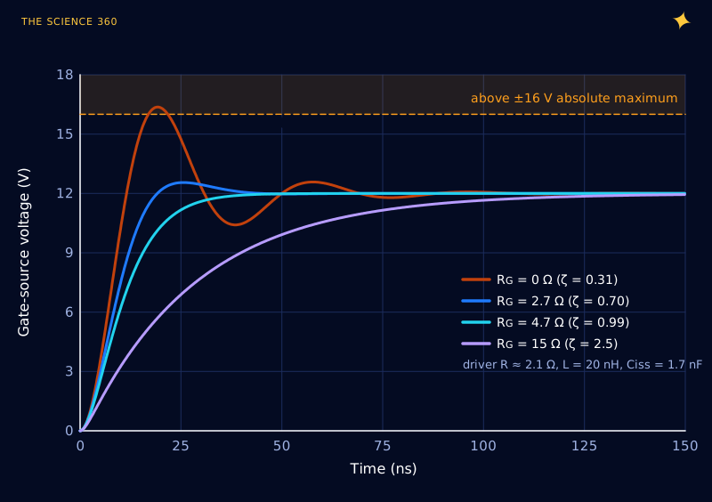
Figure 2 shows why the exact value matters less than being in the right zone. Between 2.7 Ω and 4.7 Ω the edge is fast and clean. At 0 Ω it is fast and dangerous. At 15 Ω it is safe and slow, and slow costs power.
How sensitive is this to the inductance you guessed?
The weak point of the calculation is L. You rarely know it to better than a factor of two. Fortunately the required resistance scales with √L, so a factor of two in inductance changes the answer by only 41%.
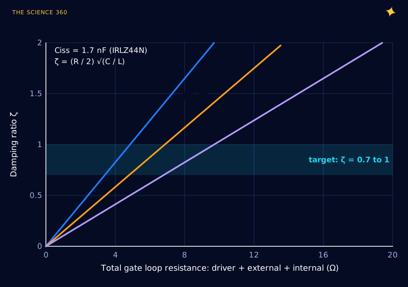
The practical procedure: compute RG for your best guess of L, build it, and look at the gate with a scope using a short ground spring on the probe. If you see ringing, increase RG one or two E12 steps. The better fix, when you can, is to shrink the loop: put the driver right next to the MOSFET and run the gate trace directly over its return.
What does a bigger gate resistor cost you?
Every ohm you add stretches the switching transition, and during the transition the MOSFET carries current and blocks voltage at the same time. The standard first-order estimate uses the charge that must move during the transition (roughly half of Qgs plus all of Qgd) and the gate current available at the Miller plateau voltage Vpl:
Gate charges from the IRLZ44N datasheet.
For a load of 12 V at 5 A, the IRLZ44N transfer curve puts Vpl near 2.7 V. One caveat: the datasheet measures Qgd at VDS = 44 V, so at 12 V the real Miller charge is smaller and these losses are on the pessimistic side.
Gate driver, RG = 4.7 Ω, 20 kHz
Compare the conduction loss at full duty: .
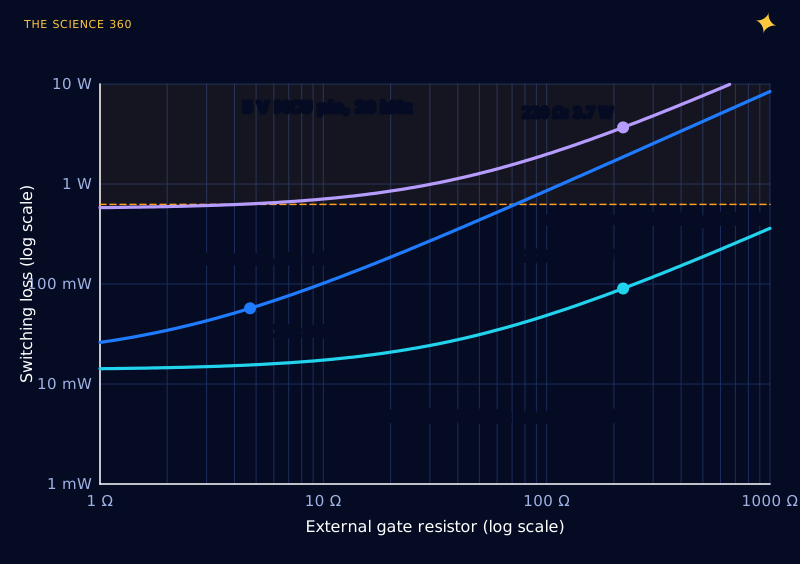
Figure 4 contains the most useful lesson in this post. With a proper driver, the gate resistor that gives good damping (a few ohms) also keeps switching loss small compared with conduction loss. From a microcontroller pin, the switching loss is dominated by the pin itself, and the only real decision is the PWM frequency. At Arduino's default 490 Hz, fine. Above a few kilohertz with amps of load, use a driver.
What gate resistor should you use with an Arduino or other microcontroller?
An ATmega328P output pin is guaranteed to hold within 0.8 V of the rail while sinking 20 mA at 5 V, which implies an output resistance of up to about 40 Ω. The per-pin absolute maximum is 40 mA DC.
Peak gate current at the moment of switching (gate at 0 V, pin at 5 V)
With no resistor the current is limited only by the pin.
Damping with 220 Ω (L = 20 nH, C = 1.7 nF)
Very overdamped, so no ringing is possible.
Switching time and loss at 490 Hz, 12 V 5 A load
Is the 125 mA spike with no resistor actually destructive? It lasts well under a microsecond and Microchip rates the pin for DC, so in practice pins usually survive it. But it is a stress you are imposing for no benefit, and it couples a sharp current spike into the microcontroller's ground. A 100 to 220 Ω resistor is the boring, correct answer. Arduino's analogWrite() runs at about 490 Hz on most Uno pins (980 Hz on pins 5 and 6), so the slower edges cost almost nothing.
One more check: logic-level drive. The IRLZ44N specifies RDS(on) at VGS = 5 V (25 mΩ) and 4 V (35 mΩ). Plenty of popular MOSFETs, like the IRFZ44N without the "L", only specify it at 10 V and will run hot from a 5 V pin no matter what resistor you choose.
Why does a MOSFET need a gate pulldown resistor?
The pulldown (10 to 100 kΩ from gate to source) is about what happens when nobody is driving. During power-up, reset or firmware flashing, microcontroller pins are high-impedance inputs. The gate, a well-insulated capacitor, will then sit at whatever voltage leakage, capacitive coupling from the drain, or a stray finger puts on it. A MOSFET half on with 12 V across it and amps available can dissipate enough to fail.
Two details that tutorials skip:
- Where it goes. Put it on the MOSFET side of the gate resistor, from gate to source. That way it holds the gate even if the series resistor or the connection to the driver is open. With 220 Ω in series and 10 kΩ to ground, the gate reaches 5 × 10,000 / 10,220 = 4.89 V, a negligible loss.
- Why it cannot replace a driver. On its own a 10 kΩ pulldown discharges 1.7 nF with a time constant of 17 µs, and the full gate charge takes longer still. It is a safety net for the undriven state, not a turn-off mechanism.
FAQ
What value gate resistor should I use for a MOSFET?
With a dedicated gate driver, choose the total loop resistance for a damping ratio of 0.7 to 1: , then subtract the driver and internal gate resistance. That usually lands between 2 and 10 Ω. Driven straight from a microcontroller pin, use 100 to 220 Ω to keep the pin current within its rating.
Do I need a gate resistor for a MOSFET driven by an Arduino?
It is strongly recommended. Without one, the gate capacitance draws a current spike limited only by the pin's own output resistance, roughly 40 Ω on an ATmega328P, which is well above the 40 mA absolute maximum per pin. A 220 Ω resistor limits the peak to about 19 mA and costs almost nothing in switching loss at the default 490 Hz PWM.
What does the pulldown resistor on a MOSFET gate do?
It holds the gate at 0 V when the driver is not driving, for example while a microcontroller is in reset and its pins are high-impedance inputs. Without it the gate can float or charge from leakage and noise, half-turning the MOSFET on. Values of 10 to 100 kΩ are typical.
Why does my MOSFET gate ring?
The gate drive path has inductance from traces, leads and the package, and the MOSFET input is a capacitance. Together they form a series LC circuit that resonates, typically at tens of megahertz. If the loop resistance is too low the resonance is underdamped and the gate voltage overshoots and rings.
Related on The Science 360
Sources
- International Rectifier / Infineon, IRLZ44NPbF datasheet (Ciss 1,700 pF, Qg 48 nC, Qgs 8.6 nC, Qgd 25 nC at VDS = 44 V, LS 7.5 nH, VGS ±16 V, RDS(on) 25 mΩ at 5 V, transfer characteristics): infineon.com/dgdl/irlz44npbf.pdf
- L. Balogh, Texas Instruments SLUA618A, "Fundamentals of MOSFET and IGBT Gate Driver Circuits" (gate-drive resonant circuit, Equation 15 for RGATE,OPT): ti.com/lit/pdf/slua618
- Microchip TC4420/TC4429 6 A MOSFET driver datasheet (output resistance 2.1 Ω typ high, 1.5 Ω typ low): microchip.com/en-us/product/TC4420
- Microchip (Atmel), ATmega328P datasheet 7810D, DC characteristics (VOL 0.8 V at 20 mA, VOH 4.1 V at −20 mA, 5 V) and absolute maximum ratings (40 mA per I/O pin): ww1.microchip.com ATmega328P datasheet PDF
- Arduino language reference, analogWrite() PWM frequencies (490 Hz, 980 Hz on Uno pins 5 and 6): reference.arduino.cc analogWrite
- Altium, "PCB Trace Inductance Calculation: How Wide is Too Wide?" (typical 5 to 10 nH per inch of trace): resources.altium.com
Method note: step responses are a numerical integration of the linear series RLC equations; switching losses use the first-order gate-charge model with datasheet charges. Loop inductance is an estimate; measure your own gate waveform before finalizing a design.
Header image: NASA (image GRC-2015-C-00595), regraded for this article.