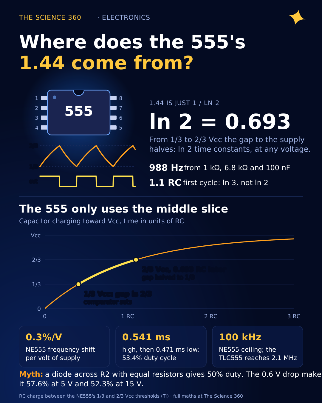
555 Timer Frequency Formula: Where 1.44 Comes From

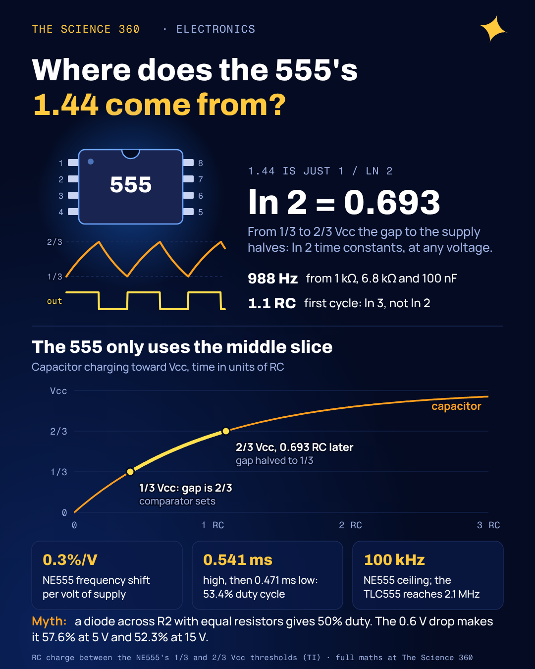
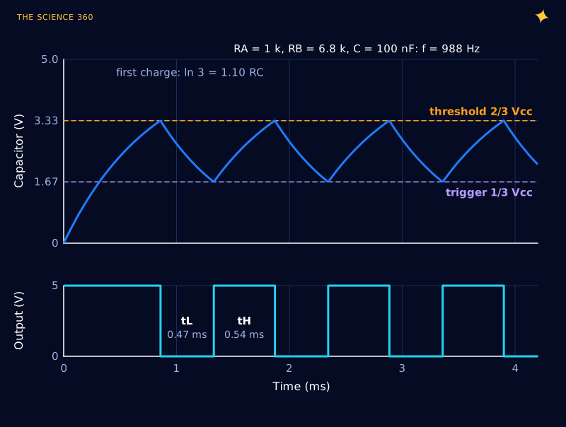
Wire a 555 with a 1 kΩ resistor, a 6.8 kΩ resistor and a 100 nF capacitor, power it from 5 V, and a scope will show a square wave at about 988 Hz. Change the supply to 12 V and the frequency barely moves. Every 555 calculator on the web will give you that number from . Almost none of them tell you where the 1.44 comes from, and that matters, because the same reasoning tells you when the formula is wrong.
The constant is not an empirical fudge. It is 1/ln 2, and it falls straight out of the two comparator thresholds at one third and two thirds of the supply. Once you see that, three things that trip people up become obvious: why the first cycle is longer than the rest, why the duty cycle cannot go below 50% in the standard circuit, and why the popular diode trick for 50% duty does not actually give 50%.
How does a 555 astable work?
Inside the chip, three equal resistors divide the supply into two reference levels, about 1/3 Vcc and 2/3 Vcc. One comparator watches the THRESHOLD pin and resets a flip-flop when the capacitor climbs above 2/3 Vcc. The other watches the TRIGGER pin and sets it when the capacitor falls below 1/3 Vcc. When the flip-flop is reset, the output goes low and an open-collector transistor on the DISCHARGE pin shorts pin 7 to ground.
In the astable circuit you tie TRIGGER and THRESHOLD together on the timing capacitor. R1 runs from Vcc to the discharge pin, R2 runs from the discharge pin to the capacitor. While the output is high, the discharge transistor is off and C charges through R1 + R2 in series. When it reaches 2/3 Vcc the transistor turns on, grounding the junction between the resistors, and C discharges through R2 alone. At 1/3 Vcc it lets go and the cycle repeats. TI's datasheet puts it plainly: the capacitor "charges through RA and RB and then discharges through RB only".
Where does 0.693 come from?
Start with the one equation you need for any RC circuit. A capacitor charging through resistance R toward a supply V closes the remaining gap exponentially:
so the time to shrink the gap by a factor k is .
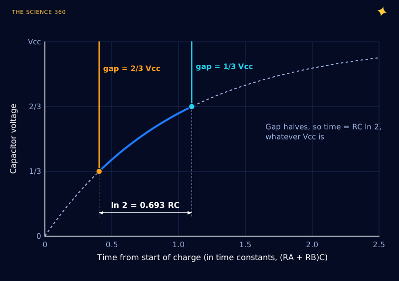
Now look at what the 555 asks of the capacitor during the high time. It starts at 1/3 Vcc, so the gap to the supply is 2/3 Vcc. It stops at 2/3 Vcc, where the gap is 1/3 Vcc. The gap has halved, so k = 2:
Discharge is the same story aimed at 0 V instead of Vcc. The voltage goes from 2/3 Vcc to 1/3 Vcc, which halves it again:
That is the whole derivation, and Figure 2 shows it as a picture. If you read the RC article on why one time constant is 63%, this is the same curve: 0.693 RC is simply the RC circuit's half-life.
Notice that Vcc cancelled out completely. Both thresholds come from the same internal divider, so they scale with the supply, and so does the charging current. That is why TI's NE555 datasheet says the charge and discharge times, and therefore the frequency and duty cycle, are "independent of the supply voltage", and specifies only a small residual sensitivity: 0.3% per volt typical in astable mode for the NE555 and 0.1% per volt for the CMOS TLC555.
The monostable formula follows the same logic. There the capacitor starts at 0 V and charges to 2/3 Vcc, so the gap goes from Vcc to Vcc/3, a factor of three. The pulse width is , which every datasheet rounds to the familiar . The same factor explains the long first cycle in Figure 1: from a dead start, the first high time is 1.1 (R1 + R2) C, not 0.693 (R1 + R2) C.
Worked example: a 1 kHz 555 oscillator
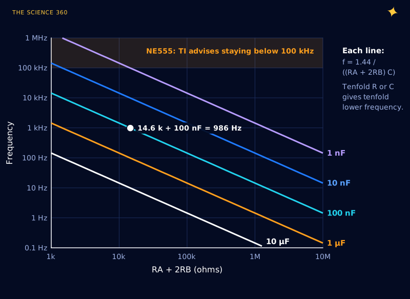
Suppose you want roughly 1 kHz with a duty cycle near 50%. Pick C first, since capacitors come in fewer values, then solve for R1 + 2R2:
Target f = 1 kHz, choose C = 100 nF.
Make R2 dominate for near-50% duty: R1 = 1 kΩ, R2 = 6.8 kΩ (E12), so R1 + 2R2 = 14.6 kΩ.
Two practical checks follow from this. The first is current: while the output is low, the discharge transistor pulls the R1/R2 junction to ground, so R1 sits directly across the supply. With R1 = 1 kΩ that is 5 mA at 5 V and 15 mA at 15 V, flowing for no reason other than to waste power. The second is the capacitor: a ceramic X7R or an electrolytic can easily be 10% to 20% off nominal, and that error goes straight into the frequency. A C0G ceramic or film capacitor fixes most of it.
The same 988 Hz with a CMOS 555 such as the TLC555 can use ten times the resistance and a tenth of the capacitance, because its threshold input draws almost nothing:
C = 10 nF (C0G), R1 = 10 kΩ, R2 = 68 kΩ, so R1 + 2R2 = 146 kΩ.
Duty is still 53.4%. Wasted current through R1 when the output is low: .
What limits the resistor and capacitor values?
The formula has no upper or lower bound in it, but the chip does. At the high-resistance end, the NE555's threshold pin draws a bias current (TI lists 30 nA typical, 250 nA maximum), and the timing resistors have to supply it on top of charging the capacitor. TI's footnote turns that into a ceiling: R1 + R2 of about 3.4 MΩ at 5 V and about 10 MΩ at 15 V. Electrolytic capacitor leakage sets a similar ceiling for long periods, which is why multi-minute 555 timers drift.
At the fast end, the formula assumes the comparators and flip-flop respond instantly. They do not. TI's TLC555 datasheet notes that the equations "do not account for any propagation delay times", which add directly to each half-period, and that the discharge transistor's on-resistance adds to R2. Its corrected equations show the logarithm drifting from ln 2 at low frequency toward ln 3 at very high frequency. The practical upshot from the datasheets:
- NE555 (bipolar): 4.5 V to 16 V supply, about 2 to 3 mA quiescent current at 5 V, TI suggests 100 kHz or below.
- TLC555 (CMOS): 2 V to 15 V supply, 180 µA typical at 5 V, typical maximum astable frequency 2.1 MHz with 470 Ω, 200 Ω and 200 pF.
The bipolar part also pulls a sharp burst of supply current every time the output switches (TI advertises the CMOS version's low current as reducing "spikes during output transitions"). That burst is why a bipolar 555 wants a local bypass capacitor right at pin 8, the job described in why 100 nF is the standard decoupling capacitor.
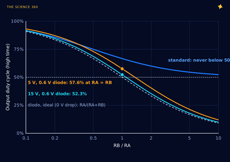
Why can’t the 555 duty cycle go below 50%?
Look at the two times again. The high time uses R1 + R2, the low time uses only R2. Since R1 must be more than zero (with R1 = 0 the discharge transistor would short Vcc to ground), the high time is always longer:
The last line approaches 50% but never reaches it.
The standard fix is a diode across R2, anode at the discharge pin, so the capacitor charges through R1 and the diode and discharges through R2. Every web calculator then tells you and , so equal resistors give exactly 50%. That is the misconception: the formula forgets the diode's forward drop.
With the diode in the charge path, the capacitor is no longer charging toward Vcc. It is charging toward Vcc minus about 0.6 V, and the gap stops halving neatly. Redo the derivation with that target:
With VD = 0.6 V:
So the multiplier is not 0.693. With R1 = R2:
At 5 V the high time is 36% longer than the textbook formula predicts. The 0.6 V figure is a typical silicon small-signal value I have assumed for illustration; a Schottky diode at 0.3 V gets closer to ideal, and the drop also changes with current and temperature, so the duty cycle wanders with them. If you want a real 50% square wave, the cleaner options are to trim R1 a little lower than R2 on the bench, or to feed a 555 output into a flip-flop that divides by two, which produces 50% by construction.
CMOS vs bipolar 555: which should you use?
For new designs, the CMOS versions are the default unless you need the bipolar part's output current. The NE555 can sink or source up to 200 mA, enough to drive a small relay directly (with a flyback diode across the coil). The TLC555 sources only about 10 mA typical but runs from 2 V, draws about a tenth of the current, accepts megohm timing resistors and runs much faster. The timing formula is identical for both, because it depends only on the 1/3 and 2/3 thresholds, which both chips share.
One caution for CMOS parts: because they are so frugal, the stray current from a long, unguarded timing node or a leaky electrolytic matters more. Keep the capacitor close to pins 2 and 6 and use a film or C0G part for anything that should hold its frequency.
FAQ
What is the formula for 555 timer frequency?
In the standard astable circuit . The high time is 0.693 (R1 + R2) C and the low time is 0.693 R2 C. The constant 0.693 is ln 2 and 1.44 is its reciprocal.
Why is 0.693 used in the 555 timer formula?
The capacitor swings between one third and two thirds of the supply. While charging from 1/3 to 2/3 Vcc the remaining gap to Vcc halves, and an RC circuit needs ln 2 = 0.693 time constants to halve any gap. Discharging from 2/3 to 1/3 Vcc also halves the voltage.
Can a 555 astable have a duty cycle below 50 percent?
Not in the standard two-resistor circuit, because the capacitor charges through R1 + R2 but discharges through R2 alone, so the high time is always longer. A diode across R2 makes lower duty cycles possible, but the diode drop lengthens the high time, so equal resistors give about 58% at 5 V rather than 50%.
Does 555 frequency depend on supply voltage?
Almost not. The thresholds and the charging rate both scale with Vcc, so the timing cancels out. TI specifies a typical astable supply sensitivity of 0.3% per volt for the NE555 and 0.1% per volt for the CMOS TLC555.
Why is the 555 monostable pulse 1.1 RC?
In monostable mode the capacitor starts at 0 V and charges to 2/3 Vcc. The remaining gap goes from Vcc to Vcc/3, a factor of three, which takes ln 3 = 1.0986 time constants. Rounded, that is 1.1 RC.
Related on The Science 360
Sources
- Texas Instruments, NA555/NE555/SA555/SE555 datasheet, SLFS022K (astable equations, 1/3 and 2/3 thresholds, "independent of the supply voltage", 100 kHz guidance, supply sensitivity 0.3%/V astable, 3.4 MΩ and 10 MΩ resistor limits, 4.5 V to 16 V supply): ti.com/lit/ds/symlink/ne555.pdf
- Texas Instruments, TLC555 LinCMOS timer datasheet, SLFS043K (2 V to 15 V, 180 µA typical at 5 V, 2.1 MHz typical maximum astable frequency, propagation-delay and on-resistance correction with ln 2 to ln 3 limits, tw = 1.1 RC): ti.com/lit/ds/symlink/tlc555.pdf
- Adafruit Learning System, "Getting to know the 555: Astable" (charge through both resistors, discharge through one): learn.adafruit.com/getting-to-know-the-555/astable
- All About Circuits forum, "555 RC time constant formula question" (common confusion about where 1.44 and 0.693 come from): forum.allaboutcircuits.com/threads/555-rc-time-constant-formula-question.71361
Method note: all curves are computed from the exponential RC equations with ideal 1/3 and 2/3 Vcc thresholds. The diode-steered duty cycles assume a fixed 0.6 V forward drop, an illustrative value rather than a datasheet figure for a specific diode.
Header image: NASA/JPL-Caltech (image PIA21085), regraded for this article.