Button Debounce Capacitor Value: How to Size the RC

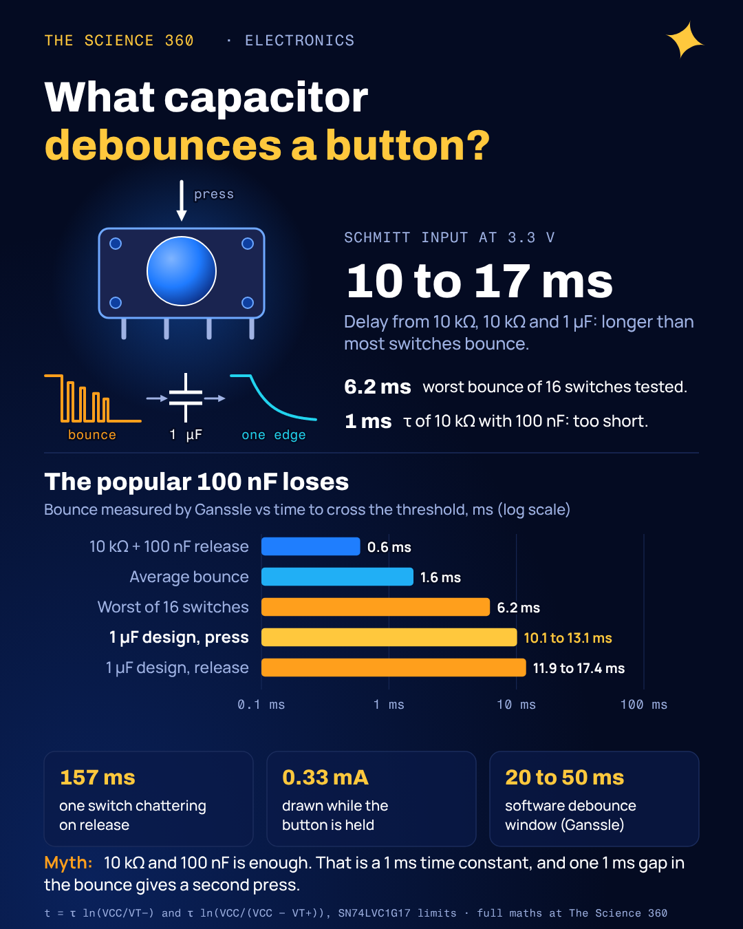
Jack Ganssle once wired 18 different switches to a logic analyzer and pressed each of them hundreds of times. Sixteen of them bounced for an average of 1.6 ms. The worst of those hit 6.2 ms. One red pushbutton, on release, chattered for 157 ms, about a sixth of a second. That spread is the whole problem with "just put a 100 nF capacitor across it": the right value depends on what your switch actually does, and on the input it feeds.
The forum threads that rank for this question are full of numbers (100 nF, 1 µF, 10 ms) with little reasoning attached. This post builds the value from the bounce data and the logic thresholds, shows why the popular 10 kΩ and 100 nF pair is too fast for many switches, and explains the resistor that most quick fixes leave out.
How long does a button bounce?
When metal contacts close, they hit, rebound and hit again, often several times, before they settle. Opening is not clean either: the contact resistance can rise gradually and break into bursts. Ganssle's "A Guide to Debouncing" is still the best public dataset, and it is worth reading the numbers as a distribution rather than one figure:
One switch, one actuation: 11.3 ms to close fully; all its others under 10 ms
Switch E: never over 20 µs when closing, but 157 ms worst case when opening
Sub-100 ns spikes: "common"
Three lessons fall out. Bounce on press and bounce on release are different, sometimes wildly. Identical switches differ (Ganssle found matched pairs varying by a factor of two). And averages are useless for design: the debouncer has to survive the bad presses, not the typical ones. His own advice is blunt: "Assume things are worse than shown."
What does the RC debounce circuit actually do?
The circuit that works has three parts. A pull-up resistor R1 runs from VCC to the switch, which goes to ground. A second resistor R2 runs from the switch to the capacitor C, and the capacitor node drives a Schmitt-trigger input. Ganssle describes the same arrangement: the capacitor charges through R1 + R2 when the switch opens and discharges through R2 when it closes.
The capacitor is a low-pass filter on the switch. Each brief contact closure pulls its voltage down only a little, each brief opening lets it creep back only a little, and the voltage only crosses the logic threshold once the switch has stayed put for long enough. That "long enough" is what you are designing, and it comes from the same exponential covered in why the RC time constant is 63%.
Why the input must have hysteresis
An RC filter turns fast edges into slow ramps. That is exactly what an ordinary logic input hates. A plain CMOS input has one switching point, and a ramp that crawls through it lets every bit of noise flip the output back and forth. Ganssle again: "Never run the cap directly to the input on a microprocessor, or to pretty much any I/O device." A Schmitt trigger fixes this with two thresholds, a higher one for rising signals (VT+) and a lower one for falling signals (VT−). Once the output has switched, the input has to travel all the way to the other threshold to switch it back.
TI's single-gate Schmitt buffer, the SN74LVC1G17, is the part TI recommends in its debounce note. Its datasheet limits at VCC = 3 V are:
Many microcontrollers do have a Schmitt trigger in their input path these days. The ATmega328P datasheet, for example, draws one in its port schematic. But its DC table guarantees only that an input below 0.3 VCC reads low and one above 0.6 VCC reads high; it gives no hysteresis figure for ordinary I/O pins. If you design around a microcontroller pin, use those guaranteed limits.
How to calculate the debounce delay from R, C and the thresholds
The two directions are separate exponentials. On press, the capacitor discharges from VCC toward 0 through R2. On release, it charges from 0 toward VCC through R1 + R2. Each crosses its threshold at a time set by a logarithm:
Press (falling):
Release (rising):
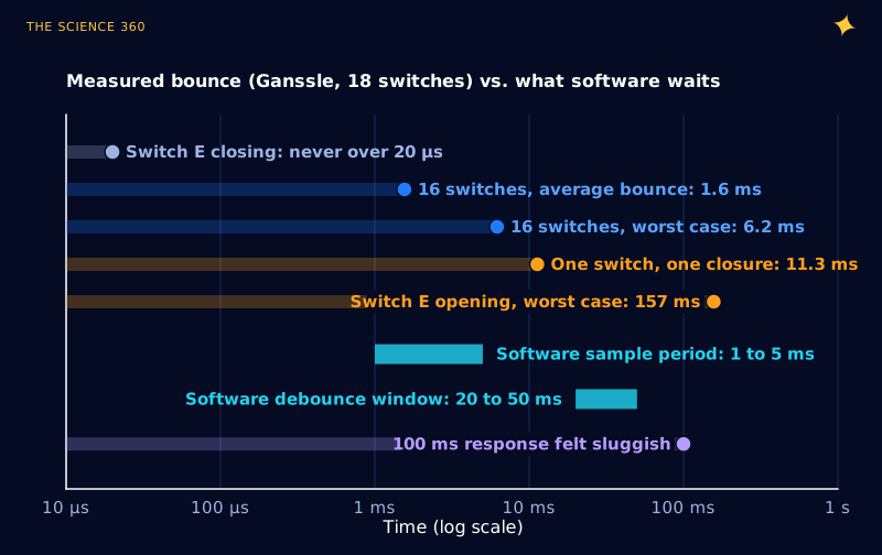
These assume the switch is perfectly closed or open for the whole interval, which is the worst case: real bounce only slows the capacitor down, so the true delay is a little longer (Figure 2 crosses at about 13.8 ms after first contact, not 10 to 13 ms).
Worked example: the recommended values at 3.3 V. I use the datasheet's 3 V threshold limits as an approximation, since TI does not list 3.3 V separately and the thresholds rise slightly with VCC. Aim for at least 10 ms in both directions, which covers every switch in Ganssle's 16-switch group with margin.
Press: need at least 10 ms at the worst (highest) .
Choose C = 1 µF and R2 = 10 kΩ, so τ = 10 ms:
Release: need at least 10 ms at the lowest .
R1 = 10 kΩ, so R1 + R2 = 20 kΩ and τ = 20 ms:
Check the housekeeping. With the button held, the only DC path is through R1: , fine for anything not running from a coin cell. The SN74LVC1G17's input leakage is at most ±5 µA, which across 20 kΩ shifts the idle voltage by 0.1 V, far from either threshold. Ganssle rejected a 180 kΩ design for exactly this reason: with about 1 µA of leakage it would have sat 0.18 V off the rail, too close to a 0.5 V switching point. Keep resistors in the tens of kilohms, as you would when choosing a pull-up resistor value.
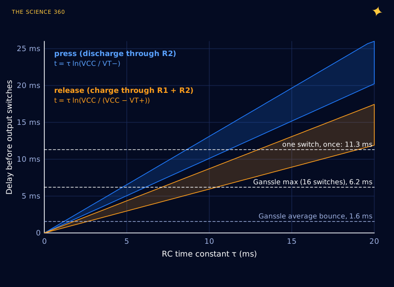
Figure 3 also tests a rule of thumb. TI's one-page debounce note says the "time constant should be approximately half of the desired debounce time" and suggests 10 ms as a common choice. With these thresholds the crossing actually happens at 0.6 to 1.3 τ, not 2 τ, so a 10 ms time constant gives 6 to 13 ms of protection, not 20 ms. The rule is a reasonable starting point. The logarithm tells you what you actually built.
Is 10 kΩ and 100 nF enough to debounce a button?
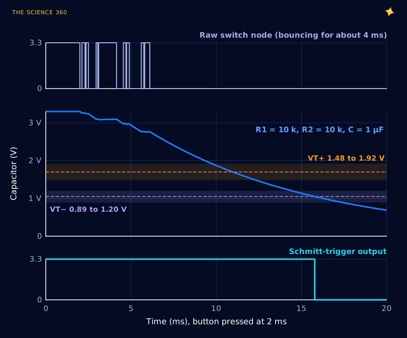
It is a common suggestion in forum answers, and it is the misconception worth correcting. Put 100 nF directly across the button with a 10 kΩ pull-up and you get a 1 ms charge time constant and essentially no discharge time constant at all. Run the numbers:
Press: the contacts short the capacitor, so τ ≈ contact resistance × 100 nF, which is nanoseconds. Compare Ganssle's average bounce of 1.6 ms and worst case of 6.2 ms.
Any gap in the bounce longer than about 0.6 to 0.9 ms lets the capacitor climb back above VT+, and the output toggles. Figure 4 shows exactly that with the same bounce pattern as Figure 2: one 1 ms gap produces a second press. Ganssle measured a switch that sat high for a few microseconds then low for about 2 ms in the middle of its bounce, so this is not a contrived case.
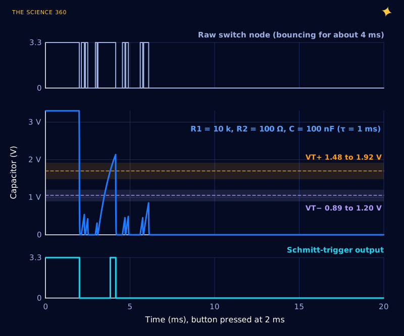
Scaling C up to 1 µF with the same 10 kΩ fixes the timing but makes the second problem worse.
Why you need a series resistor between the switch and the capacitor
With the capacitor directly across the contacts, every bounce closure dumps its charge through the contacts. The only things limiting that current are the contact resistance and the capacitor's ESR, both in the milliohm range. Ganssle's R2 exists to limit "the current through the switch contacts so a surge from the capacitor doesn't damage them," and it also keeps the discharge slow enough to filter the press side, which a bare capacitor cannot do.
Without R2 (my estimate, assuming 0.1 Ω of contact resistance plus ESR):
The 33 A lasts a fraction of a microsecond, and the 5.4 µJ is delivered at every bounce. With R2 = 10 kΩ:
A few microjoules will not weld a tactile switch, but repeated sharp current spikes erode contact plating and radiate a fast edge into everything nearby. The same reasoning makes you put a resistor in series with a MOSFET gate (see choosing a MOSFET gate resistor value). It costs one part.
Which capacitor type and tolerance?
Debounce timing is forgiving, but not infinitely. Ganssle notes standard resistors at ±5%, electrolytic capacitors at +80/−20% and small ceramics at ±30%. At 1 µF, an X7R ceramic is the usual choice; just remember X7R loses capacitance with DC bias, so a 6.3 V-rated part at 3.3 V may deliver noticeably less than its label. Design so the bottom of each band in Figure 3 still clears your bounce target with C 30% low. In the worked example, a 0.7 µF capacitor gives press delays of 7.1 to 9.2 ms, which still covers Ganssle's 6.2 ms worst case.
Two other cautions. Do not rely on a microcontroller's internal pull-up as R1 for timing: the ATmega328P specifies its I/O pull-up as anywhere from 20 to 50 kΩ, a 2.5 to 1 spread. And if your switch is a conductive-rubber keypad, check its closed resistance: Ganssle measured some over 200 Ω, which forms a divider with R1 and raises the "low" level.
Should you debounce in software instead?
Usually, yes, if a microcontroller is reading the button. Software costs nothing, adapts to the switch you actually bought, and avoids the threshold-tolerance problem entirely. Ganssle's recommendations are a sample period of 1 to 5 ms, a debounce window of 20 to 50 ms, and a timer interrupt rather than a delay loop. In his experience 50 ms "seemed instantaneous" and 100 ms felt noticeably slow. A minimal counter-based version, called from a 5 ms timer tick, looks like this:
// Called every 5 ms. Accepts a new state after 8 equal reads (40 ms).
static uint8_t count = 0;
static bool stable = false;       // debounced state
void debounce_tick(void) {
    bool raw = read_button_pin();
    if (raw == stable) { count = 0; return; }
    if (++count >= 8) { stable = raw; count = 0; on_button_change(stable); }
}
That is the same 5 ms tick and 40 ms stability requirement as the Eric Nelson routine Ganssle publishes. Two hardware rules still apply with software debouncing: do not wire a raw switch to an edge-triggered interrupt pin (each bounce fires the interrupt), and add a small RC anyway if the button lead is long or noisy, so the firmware only has to deal with bounce, not radio pickup.
Hardware debouncing earns its place when there is no processor (a switch driving a counter, a latch or a 555 timer trigger), when the input is an interrupt that wakes a sleeping chip, or when a reset line has to be clean before any code runs.
FAQ
What capacitor value should I use to debounce a button?
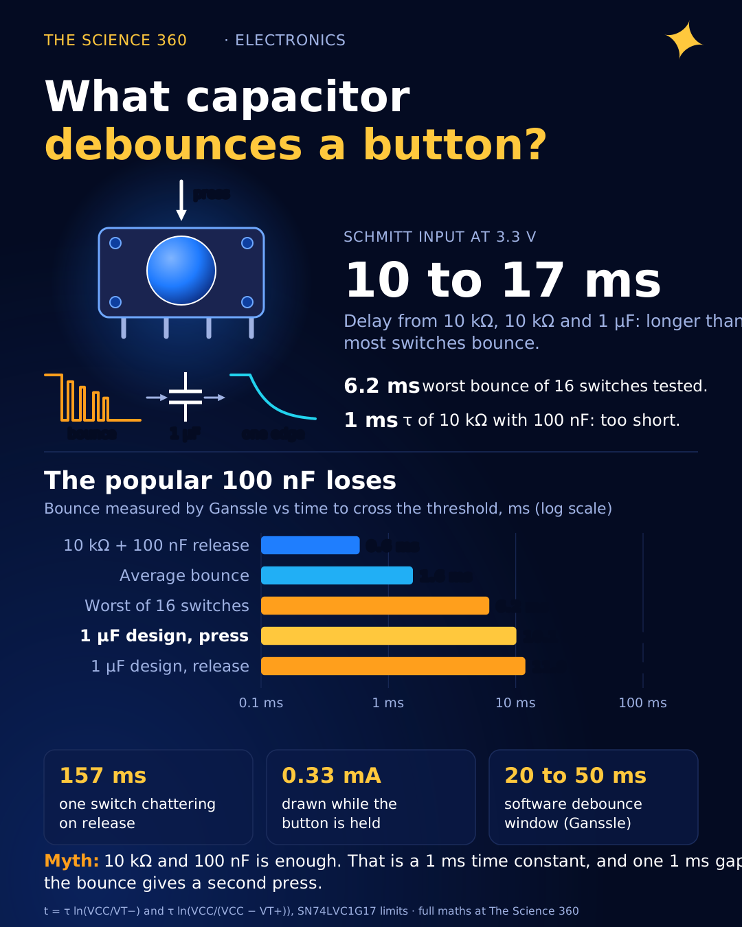
Pick the time constant first, then the capacitor. For a 3.3 V Schmitt-trigger input, a 10 kΩ pull-up, a 10 kΩ series resistor and 1 µF give a delay of about 10 to 13 ms on press and 12 to 17 ms on release, which covers the bounce of most switches. 100 nF with 10 kΩ is only a 1 ms time constant and is too short for many switches.
How long does a button bounce?
In Jack Ganssle's tests of 18 switches, 16 bounced for an average of 1.6 ms with a worst case of 6.2 ms. One switch once took 11.3 ms to close, and one bounced for 157 ms on opening. Design for 10 to 20 ms unless you have measured your own switch.
Why do I need a Schmitt trigger after a debounce capacitor?
The RC turns sharp bounces into a slow ramp. An ordinary logic input that sits on a slow ramp near its threshold can switch several times from noise alone. A Schmitt trigger has separate rising and falling thresholds, so the slow ramp produces exactly one clean edge.
Can I put a capacitor directly across a push button?
It works after a fashion but it is poor practice. Every contact closure dumps the capacitor through the contacts with only their milliohm resistance to limit the current, and the press side gets almost no filtering. A series resistor of a few kilohms between the switch and the capacitor fixes both.
What is a good software debounce time?
Jack Ganssle suggests sampling the switch every 1 to 5 ms and accepting a new state once it has been stable for 20 to 50 ms. In his tests a 50 ms response felt instantaneous and 100 ms felt sluggish.
Related on The Science 360
Sources
- Jack Ganssle, "A Guide to Debouncing", part 1 (18 switches, 1,557 µs average and 6,200 µs maximum for 16, 157 ms outlier, 11.3 ms closure, "Assume things are worse than shown"): ganssle.com/debouncing.htm
- Jack Ganssle, "A Guide to Debouncing", part 2 (R1/R2/C circuit with Schmitt trigger, contact-current role of R2, leakage problem with 180 kΩ, component tolerances, software sample period 1 to 5 ms and window 20 to 50 ms, 50 ms vs 100 ms response): ganssle.com/debouncing-pt2.htm
- Texas Instruments, SCEA094, "Debounce a Switch" (time constant about half the debounce time, 10 ms common, R and C table, SN74LVC1G17 recommendation): ti.com/lit/pdf/scea094
- Texas Instruments, SN74LVC1G17 single Schmitt-trigger buffer datasheet, SCES351Y (VT+, VT− and hysteresis limits at 3 V, ±5 µA input current): ti.com/lit/ds/symlink/sn74lvc1g17.pdf
- Microchip (Atmel), ATmega328P automotive datasheet, 7810D (input Schmitt trigger in port schematic, VIL 0.3 VCC, VIH 0.6 VCC, I/O pull-up 20 to 50 kΩ): microchip.com ATmega328P datasheet PDF
- Arduino Forum, "Debouncing capacitor" (typical page-one advice): forum.arduino.cc/t/debouncing-capacitor/868831
Method note: Figures 2 and 4 are time-step simulations of the RC network with an ideal switch and a Schmitt trigger at the midpoints of the SN74LVC1G17 3 V threshold ranges (1.70 V and 1.05 V). The bounce pattern is invented to resemble Ganssle's captures, not copied from them.
Header image: NASA/Jim Grossmann (image KSC-2011-8368), regraded for this article.