555 Timer Astable Circuit Explained with Waveforms
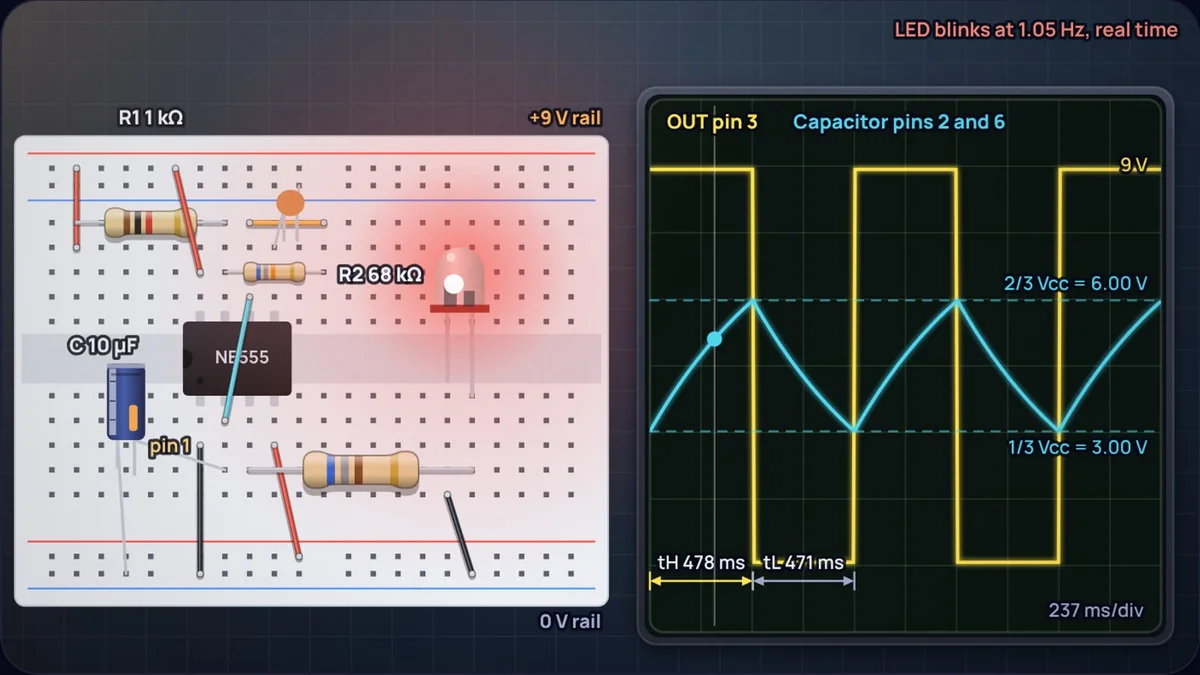
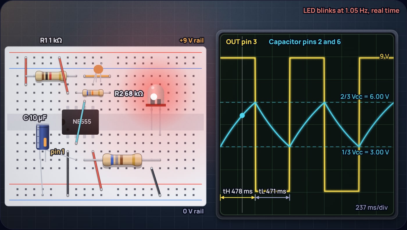
Wire up an NE555 with a 1 kΩ resistor, a 68 kΩ resistor and a 10 µF capacitor on a 9 V battery, and an LED on pin 3 blinks almost exactly once a second: on for 478 ms, off for 471 ms. Put a scope probe on the capacitor and you will see something less obvious. The capacitor never empties and never fills. It rocks between 3 V and 6 V for as long as the battery lasts, and every turnaround is an edge on the output.
This post walks through that circuit pin by pin, shows what both waveforms mean, and works through the parts choice with real numbers. Every figure comes from our 555 timer calculator and astable simulator, which draws the circuit on a breadboard or as a schematic and runs the scope at the real rate. If you want the derivation of 0.693 and 1.44 itself, that lives in where the 555 frequency formula comes from.
What does each pin of the 555 do in an astable circuit?
The NE555 is a pair of comparators, a flip-flop, an output driver and one discharge transistor, in an 8-pin package. Three equal internal resistors divide the supply to make the two reference levels, 1/3 Vcc and 2/3 Vcc. In the astable connection every pin has a fixed job:
| Pin | Name | Astable connection | What it does |
|---|---|---|---|
| 1 | GND | 0 V | Ground reference for everything |
| 2 | TRIG | To the capacitor | Starts a high phase when the capacitor falls below 1/3 Vcc |
| 3 | OUT | To the load (LED and resistor) | The square wave, sources or sinks up to 200 mA |
| 4 | RESET | To Vcc | Forces the output low when pulled low; must not float |
| 5 | CONT | 10 nF to ground | The 2/3 Vcc reference; the capacitor keeps noise off it |
| 6 | THRES | To the capacitor | Ends a high phase when the capacitor rises above 2/3 Vcc |
| 7 | DISCH | Junction of R1 and R2 | Open while the output is high, shorted to ground while low |
| 8 | VCC | Supply, 4.5 V to 16 V | Powers the chip; wants a 100 nF capacitor right at the pin |
Two resistors and one capacitor do the timing. R1 runs from Vcc to pin 7. R2 runs from pin 7 to the capacitor. Pins 2 and 6 are tied together on the capacitor's positive end. That single wire from pin 6 to pin 2 is the difference between a one-shot timer and an oscillator: the capacitor voltage now switches the chip on and off by itself.
What happens during one cycle?
Follow the capacitor round once, starting just after the output has gone high.
High phase. The flip-flop is set, pin 3 is high and the discharge transistor on pin 7 is off, so pin 7 is just a connection between R1 and R2. Current flows from Vcc through R1, then R2, into the capacitor. The capacitor started this phase at 1/3 Vcc and climbs along the usual RC curve with time constant . In Figure 1 that is the rising cyan segment while the yellow trace sits high.
The switch at 2/3 Vcc. When the capacitor reaches 2/3 Vcc the threshold comparator trips, the flip-flop resets, pin 3 drops low and the discharge transistor turns on. Pin 7 is now a short to ground.
Low phase. The capacitor discharges into pin 7 through R2 only, with time constant . R1 is not idle, though: it now sits directly across the supply, from Vcc to the grounded pin 7. That current does nothing useful, and it is why R1 should not be tiny.
The switch at 1/3 Vcc. When the capacitor falls to 1/3 Vcc the trigger comparator trips, the flip-flop sets, the output goes high, pin 7 lets go, and the high phase starts again.
In each phase the capacitor covers the part of its exponential where the gap to its target halves (from a gap of 2/3 Vcc to 1/3 Vcc while charging, from 2/3 Vcc to 1/3 Vcc while discharging toward zero). Halving a gap takes time constants, which gives the datasheet equations:
Because the thresholds and the charging current both scale with Vcc, the supply cancels. TI's datasheet says the charge and discharge times are "independent of the supply voltage". Slide Vcc in the simulator from 5 V to 15 V and the dashed threshold lines move while the frequency readout stays put.
Worked example: the 1 Hz LED flasher
Here is the circuit in Figure 1, worked through with real numbers on a 9 V battery.
R1 = 1 kΩ, R2 = 68 kΩ, C = 10 µF, Vcc = 9 V.
The thresholds are 3.00 V and 6.00 V. The first flash after power-up is longer, because the capacitor starts from 0 V: .
R2 is 68 times R1, which is what pulls the duty so close to 50%. The price is the R1 current during the low phase: for half of every second, about as much as the LED itself. On a 9 V battery that matters. Scaling both resistors up by ten and the capacitor down by ten (10 kΩ, 680 kΩ, 1 µF) gives the same 1.05 Hz with 0.9 mA wasted.
The LED hangs off pin 3 through a 680 Ω resistor. The bipolar NE555's high output sits a volt or two below Vcc (the datasheet gives 3.3 V typical at 5 V and 100 mA), so with 9 V the LED gets roughly (9 − 1.7 − 2.0)/680 Ω, about 8 mA. If you are unsure about LED resistor values, the LED resistor guide has the full table.
How do you read the 555 waveforms?
The two traces in every figure here tell you almost everything about a running 555.
- The output (yellow) is a rectangle. Its high width is , its low width is , and the high width is always the longer one in this circuit.
- The capacitor (cyan) is a curved sawtooth between the dashed 1/3 and 2/3 Vcc lines. Rising segments are charging through R1 + R2; falling segments are discharging through R2.
- The corners line up. Every peak of the cyan trace sits exactly above a falling output edge, and every valley under a rising edge. If they do not, the probe is on the wrong pin.
- The slopes tell you the resistor ratio. A rise that is much slower than the fall means R1 is large compared with R2, and the duty is high.
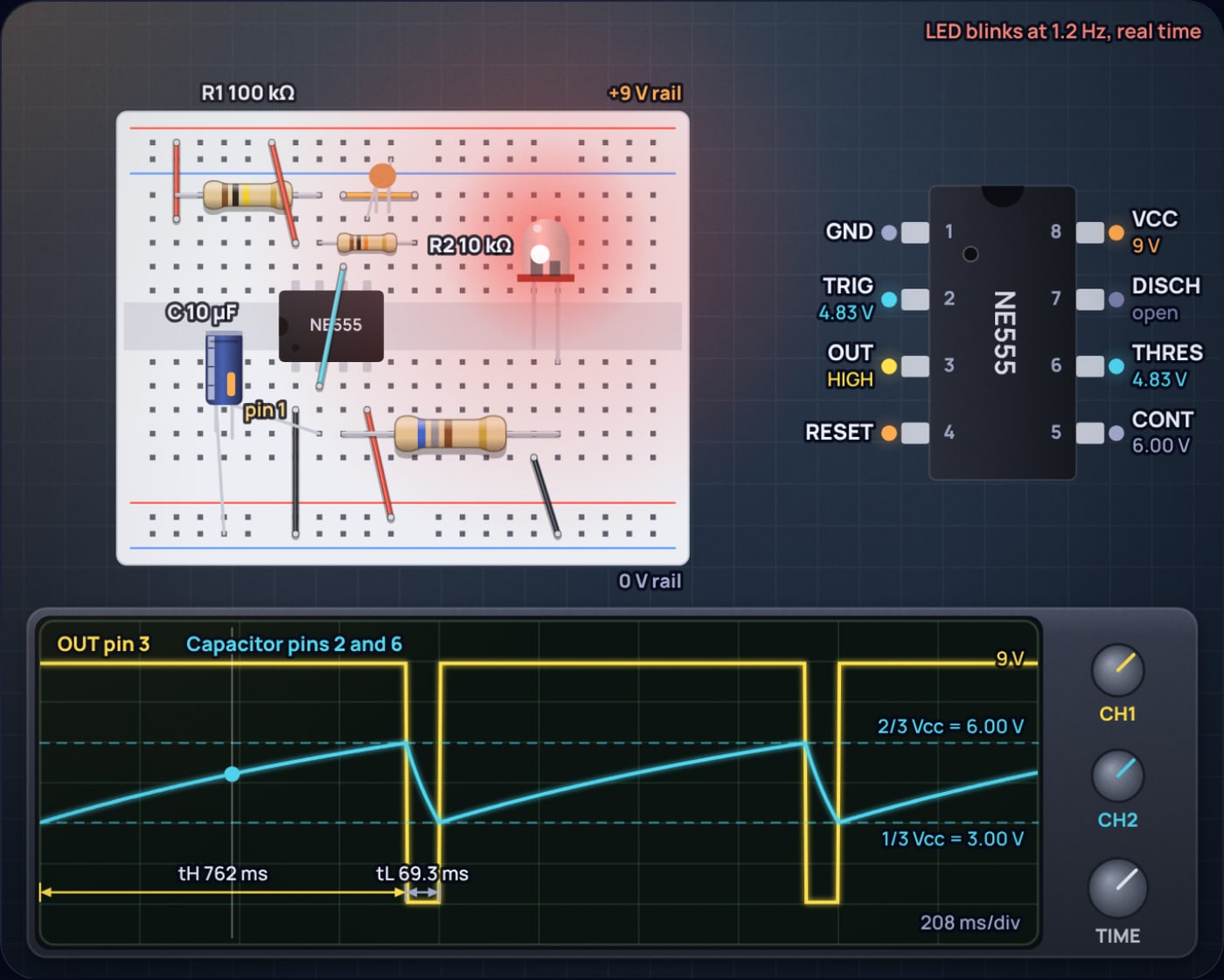
Figure 3 shows the extreme case. With R1 = 100 kΩ and R2 = 10 kΩ the capacitor crawls up for 762 ms and drops in 69 ms, so the LED is on 91.7% of the time and just winks off.
How do you choose R1, R2 and C for a target frequency?
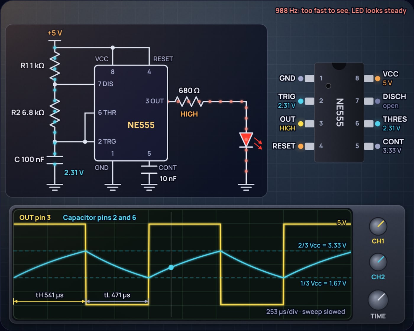
Work backwards from the times you want. If the period is T and the duty is D (the fraction of time high), then and . Choose the capacitor first, because capacitors come in fewer values, and solve for the resistors.
Target: 2 Hz with the LED on 75% of the time. So T = 0.5 s, tH = 0.375 s, tL = 0.125 s. Try C = 6.8 µF.
Round to E12 values: R1 = 56 kΩ, R2 = 27 kΩ. Check:
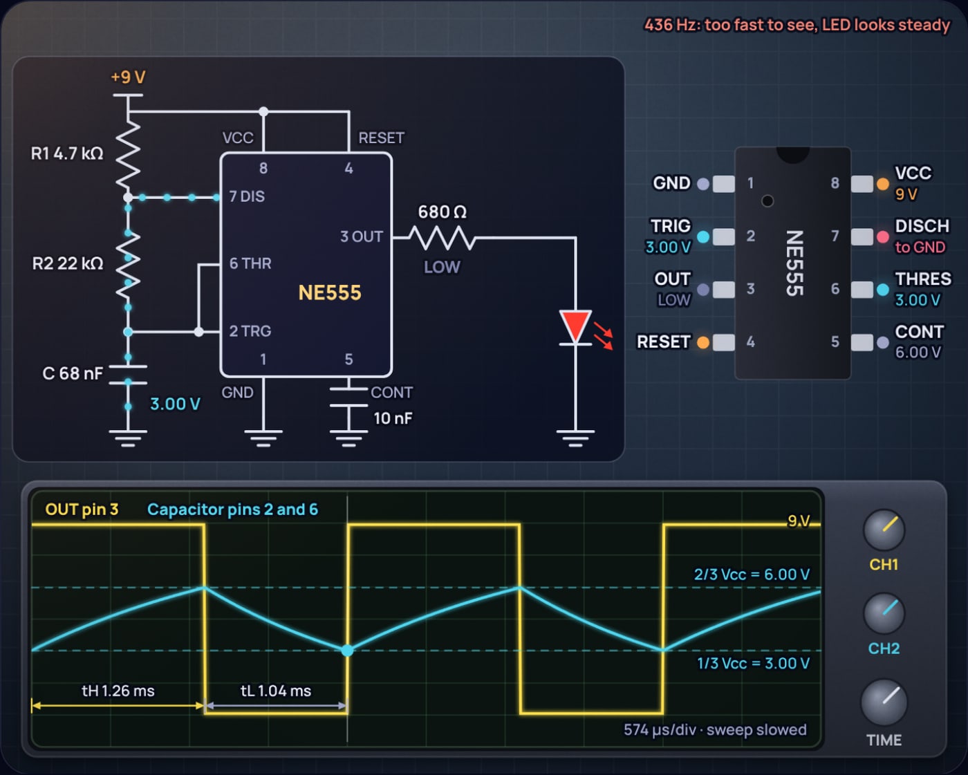
That is 3.5% slow, from rounding alone, before the capacitor's own tolerance. The simulator's Frequency → parts mode does this search over every E6 capacitor and picks the combination that lands closest, keeping R1 at 1 kΩ or more and R1 + R2 under 1 MΩ. Figure 4 shows it designing a 440 Hz tone.
Some rules of thumb for the values, mostly from TI's NE555 datasheet:
- Keep R1 at 1 kΩ or more. The datasheet's own test circuits use 1 kΩ to 100 kΩ.
- Keep R1 + R2 below about 3.4 MΩ at 5 V (about 10 MΩ at 15 V). Above that, the threshold pin's input current upsets the timing.
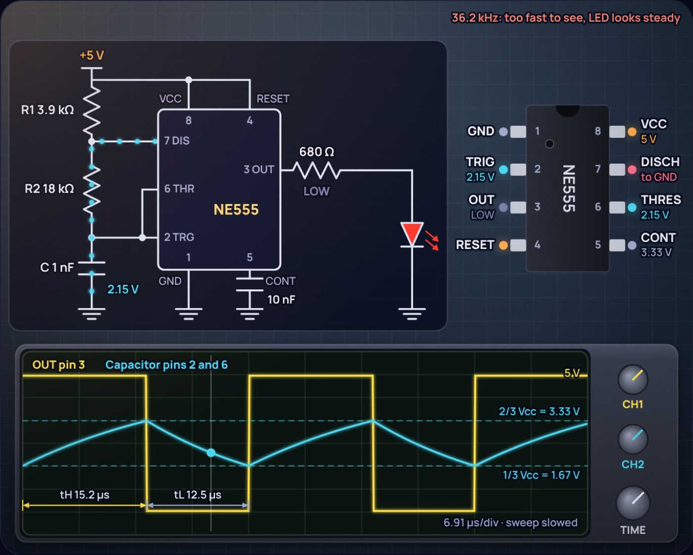
- Stay below about 100 kHz. TI suggests the CMOS TLC555 for anything faster.
- For stable timing use a film or C0G ceramic capacitor. Electrolytics are fine for blinkers but are often ±20%, and the frequency moves with them.
How do you build it on a breadboard?
The breadboard view in Figure 1 is a layout that works. Straddle the chip across the centre channel with the notch to the left, so pin 1 is bottom left. Then:
- Run red jumpers from pin 8 and pin 4 to the positive rail, and a black jumper from pin 1 to the negative rail.
- Put R1 from the positive rail to the pin 7 column.
- Put R2 from the pin 7 column to a free column, and jumper that column back to pin 6.
- Jumper pin 6 to pin 2 across the chip.
- Put the timing capacitor from the pin 2 column to the negative rail, with the stripe (negative lead) on the rail.
- Put 10 nF from pin 5 to the negative rail, and 100 nF across the supply right next to pin 8.
- Run the LED resistor from pin 3 to the LED anode, and the LED cathode to the negative rail.
The 100 nF at pin 8 is not optional with the bipolar NE555. It pulls a sharp burst of supply current at every output edge, and without a local capacitor that burst can glitch the chip or anything sharing the rail. The reason is explained in why 100 nF is the standard decoupling capacitor. If the output drives a relay coil, add a flyback diode across it.
Why does my 555 astable not work?
- Output stuck low, LED dark: pin 4 is floating or connected to ground. Tie it to Vcc.
- Output stuck high: pin 6 is not connected to the capacitor, or the capacitor is huge. A 1000 µF capacitor with 68 kΩ takes about 47 seconds per half cycle.
- Frequency 10 to 20% off: almost always the capacitor tolerance. Measure it, or use a film part.
- Chip gets warm: R1 is too small, so a large current flows into pin 7 every low phase. Raise R1.
- Jittery or erratic timing: no 10 nF on pin 5, or no decoupling at pin 8.
The fastest diagnostic is a meter or scope on the capacitor. If it moves between 1/3 and 2/3 of the supply, the chip is oscillating and the problem is on the output side. If it sits still, look at pins 2, 4, 6 and 7. The capacitor curve is the same exponential described in why the RC time constant is 63%.
Try it yourself
Open the 555 timer simulator with the 2 Hz, 75% design, switch to Breadboard and watch the capacitor bar fill while the LED is on. Then drag R1 down toward 1 kΩ and see the duty fall toward 50% and the wasted current readout climb. That trade between duty, frequency and wasted current is the whole design space of the 555 astable.
Sources
- Texas Instruments, xx555 Precision Timers data sheet (SLFS022K, revised March 2026): pin functions, 4.5 V to 16 V supply, ±200 mA output, astable equations 1 to 4, 100 kHz guidance and the 3.4 MΩ resistor limit.
- The Science 360, 555 timer frequency formula: where 1.44 comes from.
Frequently asked questions
How does a 555 timer work in astable mode?
The timing capacitor charges through R1 and R2 until it reaches two thirds of the supply. Then the output goes low and pin 7 shorts the junction of the resistors to ground, so the capacitor discharges through R2 alone. At one third of the supply the output goes high again and the cycle repeats, with no input needed.
Why are pins 2 and 6 connected together in a 555 astable?
Pin 6 (threshold) ends the high phase when the capacitor reaches two thirds of Vcc and pin 2 (trigger) starts it again when the capacitor falls to one third. Tying both to the capacitor lets the capacitor voltage switch the chip in both directions, so it oscillates by itself.
What should I connect pin 4 and pin 5 to?
Connect pin 4 (reset) to Vcc. If it floats or is pulled low the output stays low. Put a 10 nF capacitor from pin 5 (control voltage) to ground. It keeps noise off the internal two thirds reference, which otherwise jitters the timing.
Why is my 555 LED always on or always off?
The usual causes are pin 4 left floating, pins 2 and 6 not joined, the timing capacitor fitted the wrong way round or a capacitor so large that one cycle takes minutes. Check pin 4 first, then measure the capacitor voltage: it should move between one third and two thirds of the supply.
What does the capacitor waveform of a 555 astable look like?
A sawtooth made of curved segments. It rises along an RC charging curve from one third to two thirds of the supply while the output is high, then falls along a discharging curve back to one third while the output is low. It never goes near 0 V or the full supply once running.
- 555 Timer Calculator and Astable Simulator Set R1, R2 and C and watch an NE555 blink an LED at the real rate, with a labelled pinout and a scope of the capacitor between 1/3 and 2/3 Vcc. Or type a frequency and get standard parts.
- Capacitor Charging Simulator: RC Curve, Current, Energy Flip a switch to charge or discharge a capacitor through a resistor and watch the voltage, the current, one to five time constants and where the energy goes.
 ADC Resolution vs Accuracy: ENOB, INL and the Reference
 Building Your Own Quadcopter Drone: Essential Parts and Specifications in India