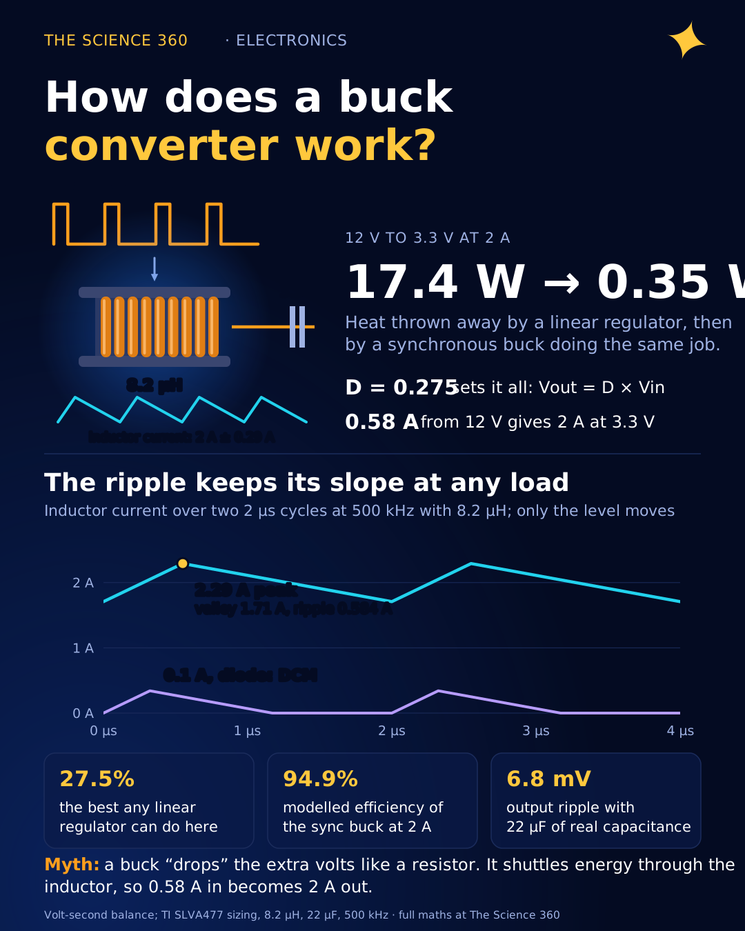
How Does a Buck Converter Work? Worked 12 V to 3.3 V

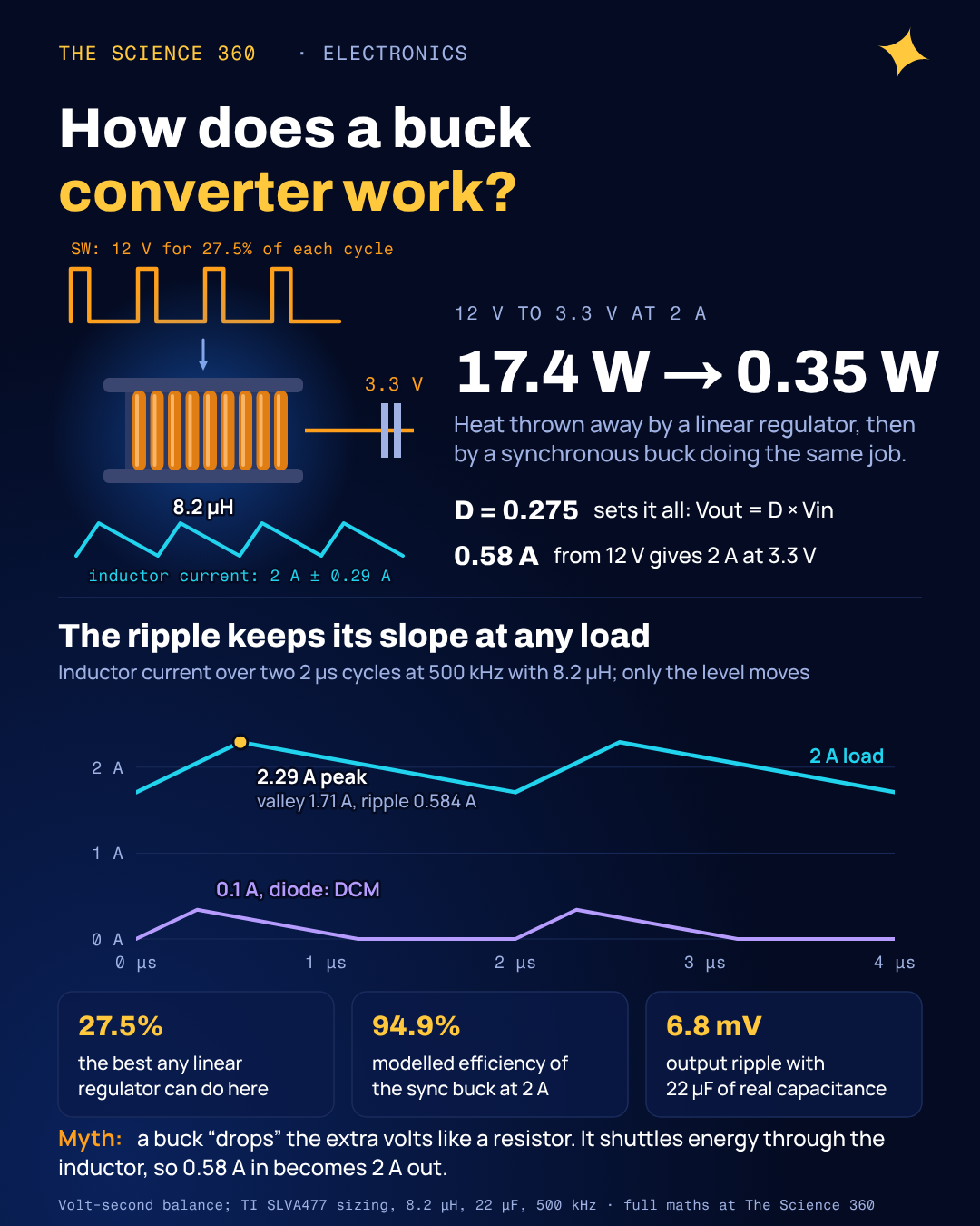
Take a 12 V supply and a board that needs 3.3 V at 2 A. A linear regulator will do it, and it will turn 17.4 W into heat while delivering 6.6 W to your circuit. That is a small electric heater bolted to your PCB. A buck converter in the same spot, built from two switches, an 8.2 µH inductor and a 22 µF capacitor, wastes around a third of a watt.
The usual explanations say the switch "chops" the voltage and a filter "averages" it. True, but it hides the one idea that makes the whole thing obvious, and it leaves out why the input current is lower than the output current. We will derive the converter from a single rule about inductors, then size a real design with numbers, and plot what every node actually does.
The circuit: two switches, an inductor and a capacitor
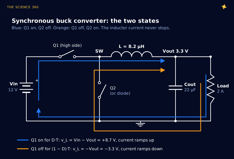
The high-side switch Q1 connects the switch node (SW) to the input. When it opens, the low-side switch Q2 closes and ties SW to ground. In a cheaper non-synchronous buck, Q2 is a Schottky diode that conducts on its own when SW tries to go negative. Either way, the switch node is a square wave between 0 V and 12 V.
The inductor sits between that square wave and the output. Its job, and this is the crux, is to refuse sudden changes in current. The voltage across an inductor sets how fast its current changes: . Apply a positive voltage and the current ramps up; apply a negative voltage and it ramps down. The current through it cannot jump, which is exactly why Q2 or the diode must exist. Open Q1 with nothing else connected and the inductor would drive the switch node as far negative as it takes to keep current flowing, usually until something breaks down. The same physics is behind the relay flyback diode.
Volt-second balance: why Vout = D × Vin
Here is the rule. In steady state, the inductor current at the end of each switching period must equal the current at the start, otherwise it would grow or shrink without limit. Since , the total change over a period is times the area under the voltage curve. Zero change means zero area: the volt-seconds the inductor gets while Q1 is on must exactly cancel the volt-seconds while Q1 is off.
Q1 on, for time DT, and Q1 off, for time (1 − D)T:
Volt-second balance:
For 12 V to 3.3 V:
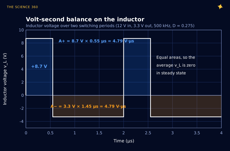
Notice what the derivation does not contain: load current, inductance, frequency. In continuous conduction the duty cycle depends only on the voltage ratio. This corrects a common intuition that you "need more on-time to deliver more current". Ideally you do not. A real controller nudges D up a little as load rises, but only to make up for resistive drops, not because the physics demands it.
Where does the extra current come from?
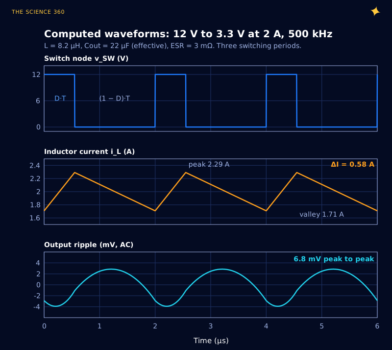
The second misconception is that a buck converter "drops" the excess voltage the way a resistor or linear regulator does. It does not. Look at Figure 1 again: during the orange interval the load is fed by the inductor and Q2, and the input supplies nothing at all. The input only delivers current during the blue interval, 27.5% of the time.
With 94.9% efficiency (Figure 5):
So the converter behaves like a DC transformer: voltage down by a factor of 3.6, current up by the same factor. If you size the 12 V supply for 2 A because "the load takes 2 A", you have overbuilt it by more than three times.
Worked design: 12 V to 3.3 V at 2 A, 500 kHz
Now let us size a real power stage, following the procedure in TI's application note SLVA477 ("Basic Calculation of a Buck Converter's Power Stage"). The note recommends choosing the inductor so the peak-to-peak ripple current is 20 to 40% of the maximum output current. We will aim for 30%.
Step 1: inductor
During the on-time the inductor current rises at for a time , which gives the ripple formula directly.
Target ΔIL = 0.30 × 2 A = 0.6 A:
Nearest standard value: 8.2 µH. Actual ripple:
The inductor must carry 2.29 A peak without saturating and about 2 A RMS without overheating. A real part such as the Coilcraft XAL6060-822 (8.2 µH) lists 24 mΩ typical DCR and 8.4 A saturation current, which is plenty of margin. Its copper loss at 2 A is about .
Step 2: output capacitor
The capacitor absorbs the AC part of the inductor current: the triangle above and below 2 A. The charge in one half of that triangle sets the capacitive ripple, and the ESR adds a term proportional to ΔI. SLVA477 gives both.
Target ripple: 10 mV (0.3% of 3.3 V).
Choose 22 µF effective. Capacitive ripple, then ESR ripple with a 3 mΩ ceramic:
Simulated combined waveform (Figure 3): 6.8 mV peak to peak.
The two ripple terms do not simply add, because the capacitive ripple is a series of parabolas that lags the triangular ESR ripple by a quarter cycle. That is why the computed total in Figure 3 is 6.8 mV, not 8.4 mV.
The word "effective" matters. A 22 µF X5R ceramic in a small package can lose half or more of its capacitance at 3.3 V of DC bias. Analog Devices' tutorial on the subject is titled, memorably, "Why Your 4.7 µF Capacitor Becomes a 0.33 µF Capacitor". In practice you might fit two 22 µF 0805 or 1206 parts to land at 22 µF of real capacitance. Our why 100nF decoupling capacitor post covers DC bias and ESL in more detail; the same parasitics decide how well this output capacitor works above a few MHz.
CCM vs DCM: what happens at light load
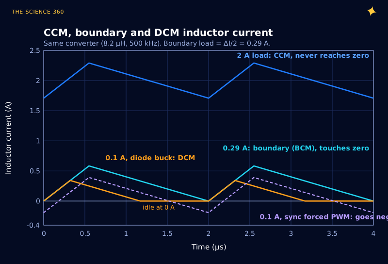
Everything so far assumed the inductor current never reaches zero, called continuous conduction mode (CCM). The triangle has a fixed height of 0.584 A regardless of load, so as the load drops, the triangle slides down. At an average of , the valley just touches zero. That is the boundary.
Below 0.29 A two things can happen, and which one depends on the low-side switch. A diode cannot conduct backwards, so the current stops at zero and sits there until the next cycle: discontinuous conduction mode (DCM). In DCM, volt-second balance still holds, but the third, idle interval changes the arithmetic and the duty cycle now depends on load.
DCM duty cycle:
At 0.1 A:
The on-time shrinks from 0.275 to 0.161. A MOSFET low-side switch, on the other hand, conducts in both directions. If the controller runs in forced PWM, the current simply goes negative for part of the cycle, the converter stays in CCM and D stays at 0.275. That keeps the frequency fixed and ripple predictable, at the cost of circulating current that does no useful work. Many modern regulators switch to a pulse-skipping or PFM mode at light load to avoid this loss.
Synchronous vs diode buck: where the watts go
The non-synchronous buck pays the diode's forward voltage every time it freewheels, and at a low output voltage it freewheels most of the time. ROHM's application material puts a Schottky's forward drop at 0.3 to 0.5 V at 1 A, against about 50 mV for a 50 mΩ MOSFET. With our numbers:
Linear regulator, for comparison:
That 27.5% is not a property of a bad regulator. It is the ceiling for any linear regulator at this ratio, since the same current flows in and out and only the voltage changes. A linear regulator here throws away 72.5% of the input power, because 8.7 of every 12 volts has nowhere to go but heat.
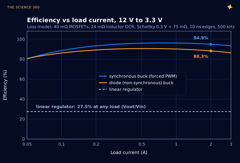
At 2 A the model gives 94.9% for the synchronous design and 88.3% for the diode version: 0.35 W against 0.88 W of loss. The gap closes at light load, where fixed losses dominate and the diode version's natural DCM helps it. That matches the industry view (DigiKey has an article titled "Nonsynchronous Buck Converters Offer Higher Efficiency at Lighter Loads"). For a 3.3 V, 2 A rail, synchronous is the default for good reason; for a 24 V to 12 V, 100 mA rail, a diode may be fine.
Practical checks before you build one
- Layout first. The input capacitor, Q1 and Q2 form a loop that carries current switching in nanoseconds. Keep it as small as possible, with the input ceramic right at the switch pins. A long loop rings and radiates.
- Peak current, not average. Check the IC's current limit and the inductor's saturation rating against the 2.29 A peak, plus margin for load transients.
- Real capacitance. Derate ceramics for DC bias at the output voltage, and remember the input capacitor sees pulses of 2.29 A, so its RMS rating matters.
- Gate drive. If you are building with discrete MOSFETs, the switching edge speed is set by the gate resistor. See how to choose a MOSFET gate resistor value.
The whole converter rests on one principle: an inductor will not let its current change suddenly, and over a full cycle its average voltage has to be zero. Everything else, the duty cycle, the ripple, the boundary of DCM and even the efficiency advantage, follows from that with a few lines of algebra.
FAQ
How does a buck converter reduce voltage?
It switches the input on and off at a fixed frequency and feeds the chopped voltage into an inductor and capacitor. In steady state the inductor's average voltage must be zero, which forces the output to equal the average of the switch node: . Energy is stored in the inductor and passed on, not burned off, so input current is lower than output current.
What is the duty cycle formula for a buck converter?
In continuous conduction, . For 12 V to 3.3 V, , so the high-side switch is on for 27.5% of each period. Real converters run slightly higher, because the controller has to make up for resistive and switching losses.
Why use a buck converter instead of a linear regulator?
A linear regulator's efficiency can never exceed Vout/Vin. From 12 V to 3.3 V at 2 A it is at best 27.5% efficient and dissipates 17.4 W as heat. A buck converter doing the same job is typically 88 to 95% efficient and wastes well under 1 W.
What happens if the inductor is too small in a buck converter?
Ripple current rises in inverse proportion to inductance. That raises the peak current (which can trip the IC's current limit or saturate the inductor), increases output voltage ripple and RMS losses, and pushes the converter into discontinuous mode at higher loads.
What is the difference between a synchronous and a non-synchronous buck converter?
A non-synchronous buck uses a Schottky diode as the low-side switch, which drops 0.3 to 0.5 V. A synchronous buck replaces it with a MOSFET that drops only tens of millivolts. At low output voltage and high current the synchronous version is several points more efficient; at very light load the diode version can be competitive.
Sources
- Brigitte Hauke, "Basic Calculation of a Buck Converter's Power Stage", Texas Instruments application note SLVA477. ti.com
- R. W. Erickson and D. Maksimović, Fundamentals of Power Electronics, chapter 2 (inductor volt-second balance), as presented in University of Liège ELEC0055 course slides. uliege.be
- ROHM TechWeb, "Differences between Synchronous and Nonsynchronous Rectifying DC-DC Conversion". techweb.rohm.com
- DigiKey, "Nonsynchronous Buck Converters Offer Higher Efficiency at Lighter Loads". digikey.com
- Coilcraft XAL6060-822 product data (8.2 µH, 24 mΩ typical DCR, 8.4 A Isat). coilcraft.com
- Mark Fortunato, "Temperature and Voltage Variation of Ceramic Capacitors, or Why Your 4.7µF Capacitor Becomes a 0.33µF Capacitor", Analog Devices. analog.com
Header image: NASA (image GRC-2000-C-00235), regraded for this article.