Transistor Base Resistor Calculation: Use Forced Beta
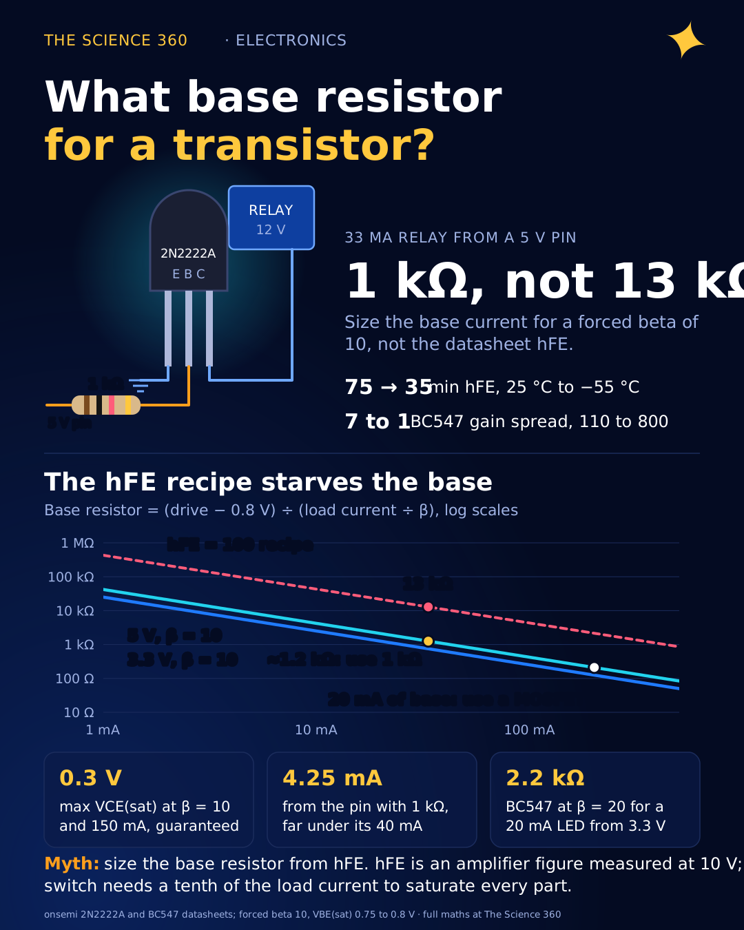
Take a 12 V relay with a 360 Ω coil, a 2N2222 and an Arduino pin. Follow the formula on most calculator pages (load current divided by an hFE of 100) and you get a 13 kΩ base resistor. Build it with a transistor whose gain sits at its guaranteed minimum and our model says the relay coil gets 8.3 V instead of 12 V, while the transistor burns 86 mW doing a job it should do for 2 mW. On a cold morning it may not click at all.
The fix is a one-line change in the recipe. Stop using the datasheet's current gain, and size the base current for a forced beta of about 10. This post shows where that number comes from, what happens to the collector voltage as base current falls, and three worked designs with real datasheet numbers.
What does the usual base resistor formula get wrong?
The formula on page one of the search results is . One calculator works a 2 mA load at a gain of 100 from 9 V and lands on 415 kΩ. Some pages add "then divide by 2 to 10 for margin", which is the right instinct with no explanation of why. Forum answers often add "use a gain of 10 for power transistors and 20 for small ones." That rule of thumb is closer to the truth than the formula it is patched onto.
The problem is what hFE means. Read the 2N2222A datasheet from onsemi and every hFE line has a test condition attached:
Three things jump out. The gain is measured with 10 V across the transistor, which is the opposite of a switch: a switch is supposed to have almost nothing across it. Dropping VCE from 10 V to 1 V halves the guaranteed gain at 150 mA. And temperature alone takes the minimum from 75 to 35. The BC547 is worse for spread: onsemi lists hFE from 110 to 800 at 2 mA for the unbinned part, a ratio above 7 between units you could pull from the same reel.
So hFE is an amplifier parameter: collector current per unit of base current when the transistor is not switched fully on. Using it to design a switch is like sizing a car's brakes from its top speed.
What is forced beta, and why 10?
When a bipolar transistor saturates, the collector current stops being set by the transistor. It is set by the load: a 360 Ω coil on 12 V can only draw however hard you drive the base. The ratio is then whatever your circuit makes it. That ratio is called the forced beta, βforced, and the transistor is saturated as long as βforced is comfortably below the gain the transistor would have in its active region. Fiore's open textbook puts the rule plainly: the ratio of saturation current to base current must be "much less than β," and "a value of 10 or so would guarantee hard saturation."
The datasheets agree, and this is the real reason for 10. The 2N2222A saturation voltages are specified at exactly that ratio:
The BC547 family uses a forced beta of 20 instead: VCE(sat) is 0.09 V typical and 0.25 V maximum at 10 mA with 0.5 mA of base current, and 0.2 V typical, 0.6 V maximum at 100 mA with 5 mA. If you drive the part at the ratio the manufacturer tested, the guaranteed maximum applies to your circuit. Drive it at a forced beta of 60 and the datasheet guarantees nothing at all.
What happens if the base current is too small?
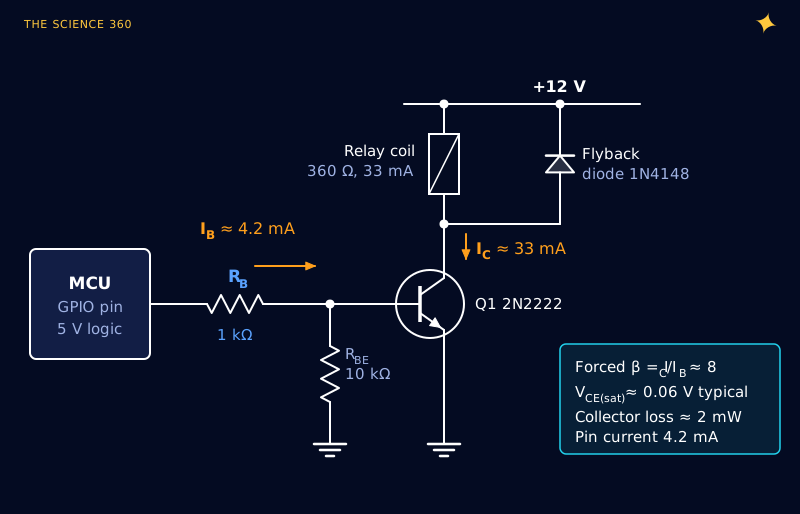
The transistor does not fail gracefully into "slightly less on." It slides out of saturation into its linear region and becomes a variable resistor sharing the supply with your load. Figure 2 shows this for the relay circuit in Figure 1. To draw it we built a small Gummel-Poon transistor model in Python (Ebers-Moll junctions plus high-injection gain roll-off and 1 Ω of collector resistance, with parameters from the widely circulated Q2N2222 SPICE model), loaded it with 360 Ω on 12 V, and solved for VCE at each base current. The three curves differ only in the transistor's low-current gain.
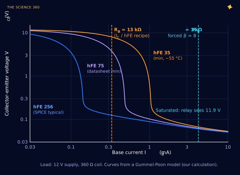
The orange dashed line is the hFE recipe's 13 kΩ resistor, which gives about 0.33 mA of base current. Read the curves where it crosses them:
Typical part (model gain 256):
Gain exactly 100:
Gain 75 (datasheet minimum at 25 °C):
Gain 35 (datasheet minimum at −55 °C):
With a gain-75 part the relay coil sees , which is 69% of its rating. Many relays need about three quarters of rated voltage to pull in reliably, so whether this circuit works becomes a lottery on the transistor and the temperature. The prototype on your bench will probably work, because a typical 2N2222 has a gain well above 100. The hundredth unit, or the one in an unheated shed, may not.
Push the base current past every knee, as the green line does, and the spread disappears. At 4.2 mA all three transistors sit between 0.060 and 0.067 V. That is the point of a switch: the outcome no longer depends on a parameter that varies 7 to 1.
How to calculate the base resistor step by step
Here is the recipe, applied to the relay driver in Figure 1.
Step 1: worst-case collector current.
Coil resistance is typically ±10%, and a cold coil reads low, so design for:
Step 2: base current at a forced beta of 10.
Step 3: voltage across RB.
at 37 mA (our model; the datasheet gives 0.6 to 1.2 V at 150 mA, so it is lower here).
Step 4: resistor.
Actual base current and forced beta:
Rounding down matters: rounding up raises the forced beta and eats the margin you designed in. Now check the parts around the resistor, because the transistor is rarely the weak link here.
Pin current: 4.25 mA. ATmega328P: absolute maximum 40 mA per pin, at 20 mA. Fine.
Low-VOH check: if the pin only reached 4.1 V:
Still saturated.
RBE = 10 kΩ steals 2% of the drive, which is negligible:
Collector dissipation:
The 2N2222A is rated 625 mW in TO-92.
Resistor dissipation:
Any 0.125 W part.
From a 3.3 V microcontroller the same steps give , so use 680 Ω, which pulls 3.75 mA from the pin. Check that your chip can source that. The batch post on how much current an Arduino pin can supply covers how the output voltage sags with load, and the reasoning is the same one we use when choosing a pull-up resistor value: the resistor has to fit the weakest pin, not the typical one. Do not leave out the flyback diode either; why a relay needs a flyback diode works through the turn-off spike you get without it.
Why does saturation voltage barely care about forced beta?
A natural worry is that a forced beta of 10 wastes current and that 30 would do. Figure 3 shows what you gain and lose. It holds the collector current at 150 mA (the datasheet test point) and raises the forced beta from 2 to 200, using the same model.
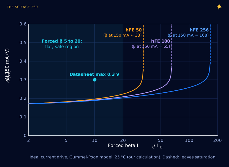
Two things are worth reading off it. First, over the shaded band from 5 to 20 the saturation voltage changes by only a few tens of millivolts: there is little to gain by driving harder than βforced = 10, and little to lose by relaxing to 15 or 20. Second, the wall arrives sooner than the hFE label suggests. A part labelled with a gain of 100 runs out at about 65 when it carries 150 mA, because gain falls at high current. That is the same effect that makes onsemi guarantee only 40 at 500 mA. A forced beta of 10 puts you below the wall for every 2N2222A the datasheet allows, at every current it specifies.
Our model gives 0.19 V at the datasheet test point against the guaranteed maximum of 0.3 V. That gap is the manufacturer's margin for process spread and is another reason not to trust a single model, ours included, for the last tenth of a volt.
Worked example: BC547 driving an LED from 3.3 V
A 20 mA indicator LED on a 5 V rail, switched by a BC547B from a 3.3 V microcontroller. The BC547 datasheet specifies saturation at a forced beta of 20, so we use that.
Actual base current and forced beta:
VCE(sat): between 0.25 V max (at 10 mA) and 0.6 V max (at 100 mA); allow 0.2 V typical.
LED resistor:
Compare the hFE recipe with the part's 200 minimum gain: IB = 0.1 mA and RB = 25 kΩ. That works for a BC547B at room temperature. Swap in an unbinned BC547 (110 minimum) or a BC547A and the LED dims noticeably, and there is no way to see why without a meter on the collector. The LED's own series resistor is a separate calculation, covered in why LEDs need a resistor.
When does a bipolar transistor stop being the right switch?
Figure 4 turns the recipe into a chart. Read across from your load current to the resistor for your drive voltage and forced beta.
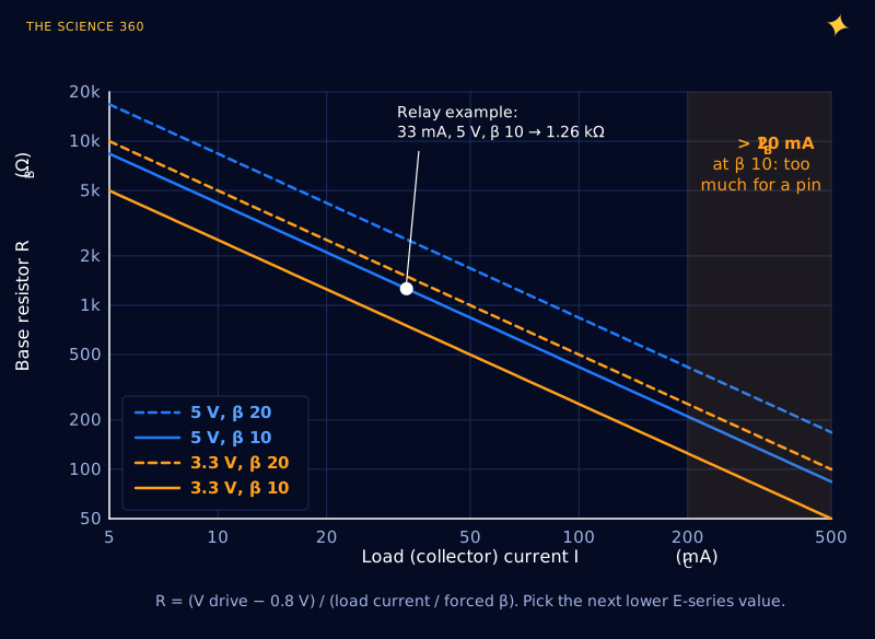
The shaded corner is where the method breaks down. Switching 500 mA with a 2N2222A at its datasheet point needs 50 mA of base current, and even then the guaranteed numbers are poor:
That is more than the ATmega328P's 40 mA absolute maximum per pin.
Temperature rise at RθJA = 200 °C/W:
That is a transistor running at 125 °C on a 25 °C bench, before any base dissipation. Past roughly 100 to 200 mA from a logic pin, a logic-level MOSFET is usually the better switch: its gate draws no steady current, and its on-resistance can be tens of milliohms. The gate still needs a series resistor for other reasons, explained in choosing a MOSFET gate resistor value. A Darlington pair solves the drive problem but not the heat, because its saturation voltage can never fall below one VBE plus the first transistor's VCE(sat), which puts it near 1 V before the load current adds anything. For bidirectional motor loads the same trade-off shows up in the H-bridge motor driver, where bipolar bridges lose several volts and MOSFET bridges lose tenths.
Does too much base current cause problems?
Within the ratings, mostly it costs speed. A heavily saturated transistor stores extra charge in its base, and that charge must be removed before the collector current can start to fall. The 2N2222A datasheet guarantees a storage time of at most 225 ns at 150 mA, and it measures that with : the base is actively pulled negative with 15 mA during turn-off. With only a resistor to ground removing the charge, expect a slower turn-off than the datasheet figure. For a relay that switches a few times a second, nobody cares. For PWM at tens of kilohertz, overdriving at βforced = 3 is a mistake, and 10 to 20 is a sensible compromise.
The other limit is the base-emitter junction's reverse rating, only 6 V on both the 2N2222A and BC547. A base driven from a 12 V square wave through a capacitor can exceed that on the negative swing. A plain logic pin through a resistor cannot.
Finally, the base-emitter resistor. During reset a microcontroller pin floats, and leakage or pickup on the base can turn the transistor partly on, so the relay chatters at power-up. 10 to 100 kΩ from base to emitter holds it off for the 75 µA calculated above. RB and RBE form a divider, the same arithmetic as in why a voltage divider is a poor power supply, so with a low RBE subtract its current from the drive.
Is a switching transistor different from an amplifying one?
Physically, no. An amplifier keeps the transistor out of saturation, where hFE and transconductance are exactly the right parameters; our companion post on how a transistor amplifies draws both regions on one load line. A switch lives in the corner of that load line where gain has stopped mattering, which is why the switch recipe should not contain the gain at all, except as a check that βforced sits well below it.
FAQ
How do you calculate the base resistor for a transistor switch?
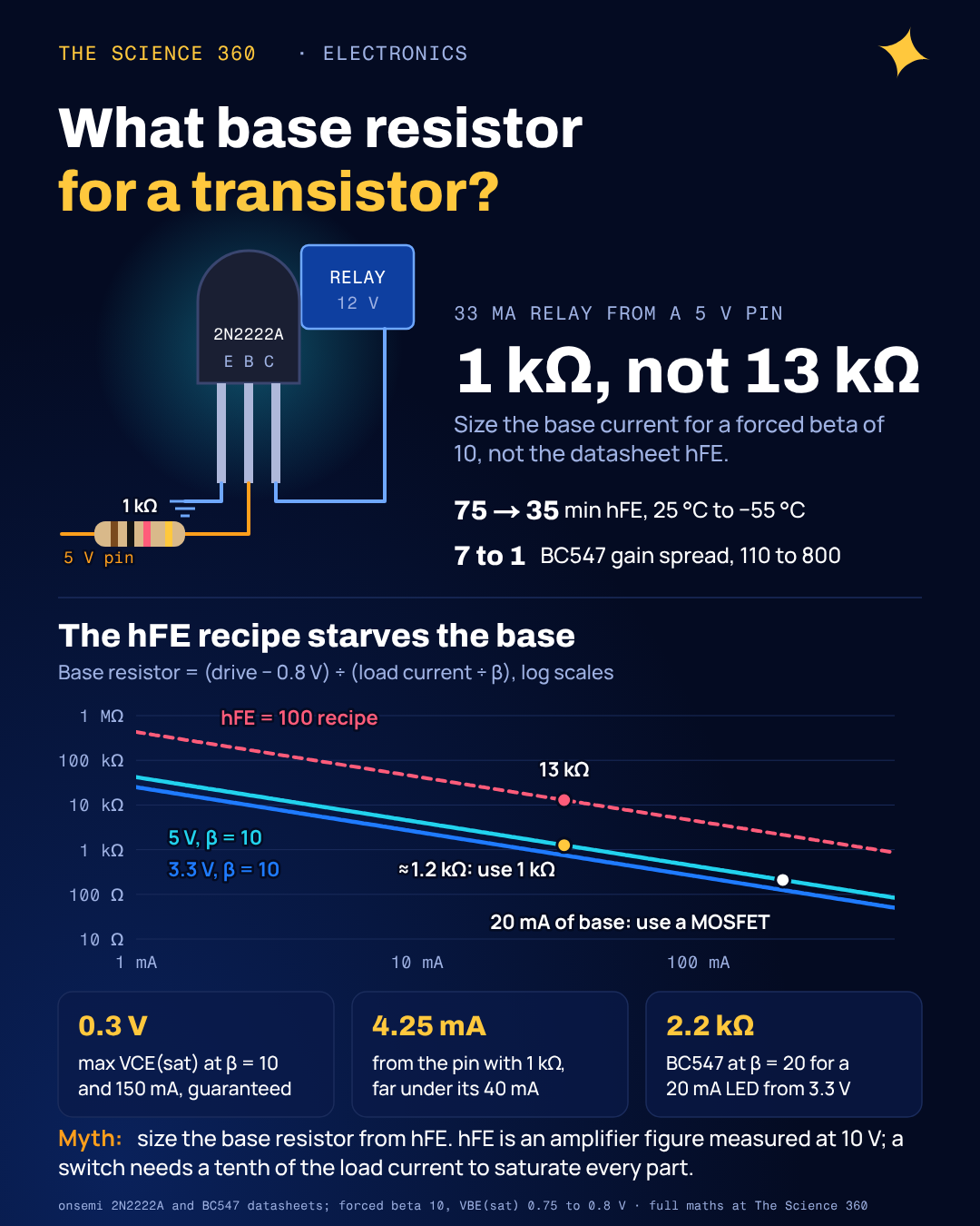
Take the worst-case load current, divide by a forced beta of 10 (or up to 20 for small-signal parts at low current) to get the base current, then divide the drive voltage minus about 0.75 to 0.9 V by that current. Round down to the next standard value. For a 33 mA relay driven from 5 V this gives about 1.2 kΩ, so use 1 kΩ.
Why not use the hFE from the datasheet to size the base resistor?
hFE is measured with the transistor out of saturation, typically at 5 or 10 V across it, and it varies by a factor of several between units and with temperature. A 2N2222A is only guaranteed 35 at −55 °C. If you size the base current from a typical hFE, many parts never saturate and drop volts instead of tenths of a volt.
What is forced beta?
Forced beta is the ratio of collector current to base current that you impose on a saturated transistor, . It is set by the circuit, not the transistor. Datasheets specify saturation voltage at forced betas of 10 or 20, so designing to those ratios lets you use the guaranteed VCE(sat) figures.
Can too much base current damage a transistor?
Within the ratings, extra base current mainly wastes drive current and slows turn-off because more charge is stored in the base. The real limits are the microcontroller pin current, the transistor's base current rating where one is given, and the base-emitter reverse voltage, which is only 6 V on parts like the 2N2222A and BC547.
Do I need a resistor from base to emitter?
It is good practice. A 10 to 100 kΩ resistor from base to emitter holds the transistor off while the microcontroller pin floats during reset or programming, and it helps remove base charge at turn-off. At 10 kΩ it steals only about 75 µA from the base drive.
Related on The Science 360
Sources
- onsemi, P2N2222A Amplifier Transistor datasheet, Rev. 7 (hFE at each test condition, VCE(sat) and VBE(sat) at , storage time 225 ns, 600 mA, 625 mW, RθJA 200 °C/W, VEBO 6 V): onsemi.com/pdf/datasheet/p2n2222a-d.pdf
- onsemi, BC546B/BC547A, B, C/BC548B, C datasheet, Rev. 8 (hFE 110 to 800, VCE(sat) 0.09/0.25 V at 10 mA/0.5 mA and 0.2/0.6 V at 100 mA/5 mA, VBE(sat) 0.7 V, 100 mA): onsemi.com/pdf/datasheet/bc546-d.pdf
- Microchip (Atmel), ATmega328P automotive datasheet 7810D (40 mA per pin absolute maximum, VOH ≥ 4.1 V at 20 mA and 5 V): microchip.com ATmega328P datasheet PDF
- James Fiore, Semiconductor Devices: Theory and Application, section 4.7 "BJT Switching and Driver Applications" (ratio "much less than β", "a value of 10 or so would guarantee hard saturation"): eng.libretexts.org
- DigiKey TechForum, "Digital Switching: Transistor Saturation and Forced Beta" (relay driver designed at ): forum.digikey.com
- Omron, G5LE PCB power relay datasheet (contact ratings; coil table not machine-readable in my copy): omronfs.omron.com G5LE PDF
- Typical page-one calculator using hFE (2 mA at gain 100 from 9 V gives 415 kΩ, "divide Rb by a factor of 2 to 10"): calculate.co.nz transistor base resistor calculator
Method note: Figures 2 and 3 come from our own Python implementation of a simplified Gummel-Poon model (no Early effect, no quasi-saturation, 25 °C) with Q2N2222 SPICE parameters, with the forward gain parameter changed to represent low- and high-gain units. Treat the curves as shape and order of magnitude, and the datasheet limits as the design numbers.
Header image: NASA (image jsc2025e015689), regraded for this article.