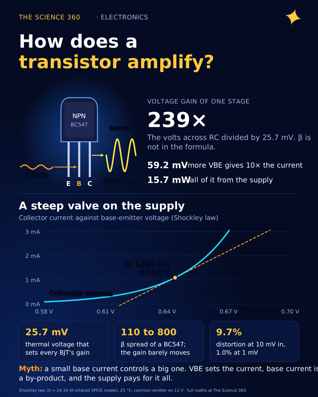
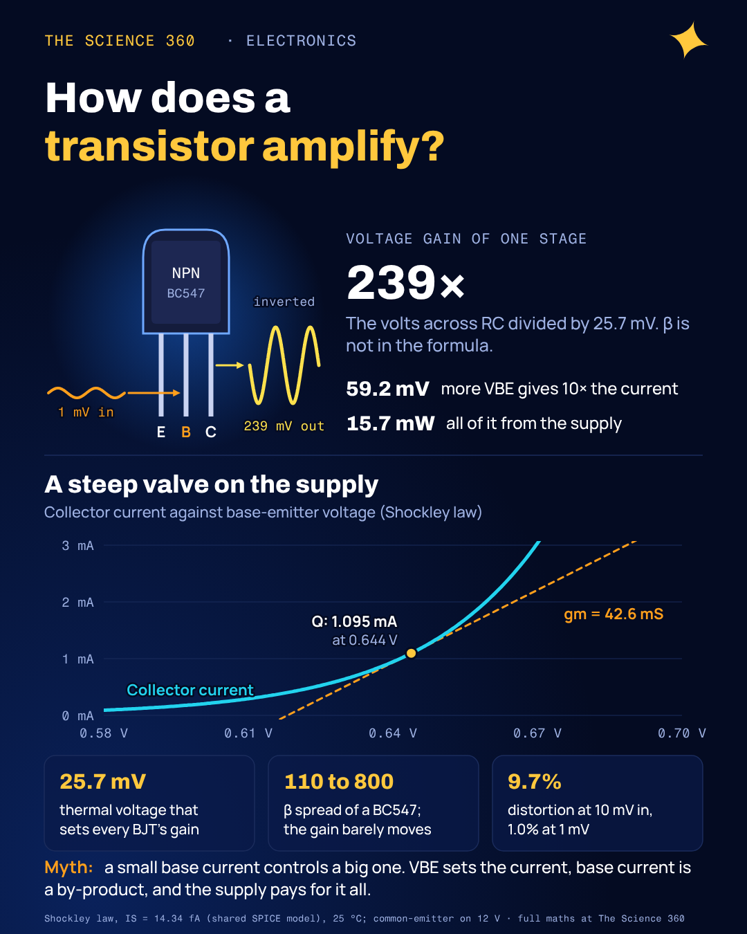
How Does a Transistor Amplify? It's a Valve, Not a Source

Put a 1 mV signal into the base of the small amplifier in Figure 3 and a 220 mV copy comes out of the collector, upside down. Measured as power, the output is about 24,000 times stronger than the input. The transistor doing this is a 3-cent part with three legs and no battery inside, which raises the obvious question: where did the extra power come from?
Most explanations on the first page of search results say "a small base current controls a larger collector current," and stop. That is true as far as it goes, but it hides the two things that actually make an amplifier work: the power supply does all the lifting, and the control is really by voltage, through an exponential law that sets the gain without any reference to the transistor's current gain. This post builds an amplifier from those two ideas, with real numbers at every step.
Does a transistor create energy?
No. A transistor is closer to a tap than a pump. The water pressure comes from the mains (the DC supply); the tap only decides how much flows. Turning a tap takes a few newtons of finger force, and the water it releases can carry far more power than your finger supplied. Nobody thinks the tap made the energy.
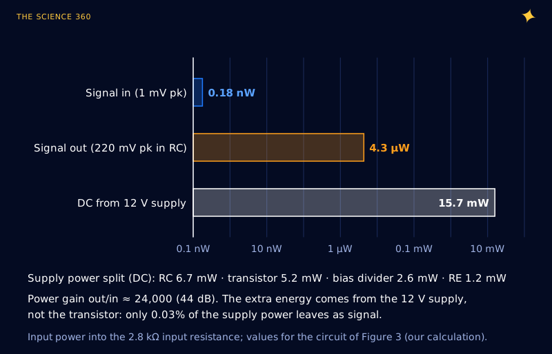
The electrical version is easy to check with the circuit in Figure 3, a textbook common-emitter stage on 12 V that we will design properly below. Here is the power budget with a 1 mV peak signal at the input:
DC power from the supply, with 1.095 mA collector current plus 0.217 mA through the bias divider:
of which: RC 6.7 mW, transistor 5.2 mW, bias divider 2.6 mW, RE 1.2 mW
Signal power in (2.8 kΩ input resistance) and out, power gain, and signal out as a share of supply power:
The signal is a ripple on a large, steady flow of supply current. The transistor's job is to make that ripple follow the input, and most of the supply power ends up as heat in the resistors and the transistor whether or not any signal is present. That is why a class A amplifier like this one is so inefficient, and why audio power amplifiers use other arrangements.
Is a transistor current-controlled or voltage-controlled?
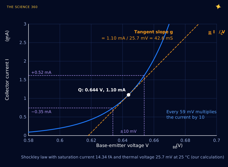
The page-one answer is "current-controlled": base current in, β times as much collector current out. It is a useful bookkeeping rule, and it is the right way to size a base resistor for a switch. But it is not the physics. In a bipolar transistor the collector current is set by the voltage across the base-emitter junction, through the same exponential law as a diode:
Raising VBE lowers the energy barrier at the emitter junction, and electrons pour from the emitter into the thin base. Almost all of them diffuse straight across it and are swept into the collector by the reverse-biased collector junction. A small fraction recombine in the base or are matched by holes flowing back into the emitter, and that leakage is the base current. Base current is the by-product, not the cause. The ratio just measures how leaky the base is, which is why it varies so much from part to part (onsemi lists the BC547 at 110 to 800).
The exponential is steep. One consequence is a number you can check on any bench:
Change in VBE for a 10× change in IC, and for a 2× change:
What is transconductance, and why is it IC/VT?
Amplifier designers care about how much the collector current changes per millivolt of input, the slope of Figure 2. That slope is called transconductance, gm. Differentiate the exponential and something neat drops out:
At IC = 1.095 mA, with the equivalent emitter resistance re:
The slope depends only on the operating current and on temperature. Not on the transistor type, not on its β, not on its size. Every silicon bipolar transistor ever made, biased at 1 mA, has a transconductance of about 39 mS at room temperature. MIT's 6.012 course notes give the same relation, , as the starting point of the small-signal model. (For comparison, a MOSFET in saturation has , where Vov is how far the gate is above threshold. At a typical 0.2 V overdrive that is 10 mS per mA, about a quarter of the bipolar figure. That is one reason bipolar transistors still turn up in low-noise and high-gain front ends.)
How does a current change become a voltage gain?
Put a resistor RC between the supply and the collector, and take the output at the collector. Collector current flows through RC, so the collector voltage is . A small input vin changes IC by , which changes the collector voltage by :
That last form is the most useful sentence in small-signal design. The voltage gain of a common-emitter stage with its emitter grounded for signals is just the DC voltage across the collector resistor divided by 25.7 mV. A Walla Walla University lab handout asks students to compare exactly this, , with what they measure. The minus sign is the inversion: input up, current up, more drop across RC, collector down.
Look at what is missing from the formula. β is not there. The current gain story says amplification comes from β, yet the voltage gain is the same for a transistor with β = 100 as for one with β = 400, provided both run at the same collector current. β matters only for the input resistance (, 4.7 kΩ here) and for how hard the bias network has to work.
The formula also sets a ceiling. On a 12 V supply you cannot put much more than half the supply across RC and still leave room for the collector to swing, so a single resistor-loaded stage tops out around . The transistor's own limit is set by its output resistance (VA is the Early voltage): the "intrinsic gain" , roughly for a 2N2222-class model. Op-amps reach gains of 100,000 or more by stacking stages and replacing resistors with current sources, then trade most of it back for accuracy, as described in our post on op-amp gain-bandwidth product.
Worked example: designing a common-emitter amplifier
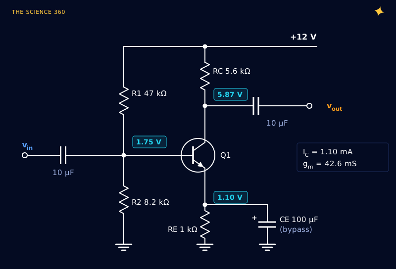
Target: about 1 mA, the collector sitting near the middle of the supply, and a bias point that does not care much about β. Supply 12 V.
Step 1, emitter resistor. Put about 1 V across RE to stabilise the current:
Step 2, collector resistor. For VC near 6 V, VRC ≈ 6 V:
Step 3, base divider. The divider current should be at least 10× the base current (5 µA at β = 200).
With R1 = 47 kΩ and R2 = 8.2 kΩ, the open-circuit VTH and RTH are:
Divider current: 0.217 mA.
Step 4, solve the loop (VBE from the exponential, iterated):
Step 5, small-signal gain.
Including ro in parallel with RC, and the input resistance:
The emitter resistor is there for stability. Run the same loop with β = 100 and with β = 400, a 4 to 1 spread typical of a reel of small-signal transistors:
Same transistors with a single 2.07 MΩ base resistor and no RE (fixed-bias, tuned for 1.1 mA at β = 200):
At β = 400, VC would be:
Saturated, no amplifier.
That is the real reason for the slightly fussy four-resistor circuit: the emitter resistor makes the collector current depend on a voltage you set with resistors, not on β. The divider is the same kind of loaded divider discussed in why a voltage divider is a poor power supply, and the rule of "divider current at least 10× the load current" is doing the same job here.
The 100 µF bypass capacitor shorts RE for signals, so the gain is set by instead of the much smaller . Capacitors only short above some frequency, and the corner frequencies follow from the familiar , as in our RC filter cutoff post:
Input coupling:
Emitter bypass: resistance seen by CE, then the corner:
This sets the low-frequency end of this amplifier.
What does the load line show?
Figure 4 plots the transistor's output characteristics, collector current against collector-emitter voltage at fixed base-emitter voltages, with the circuit's constraints drawn on top. The blue DC load line is every combination the resistors allow: 12 V shared between the transistor and . The bias network picks the point Q on it.
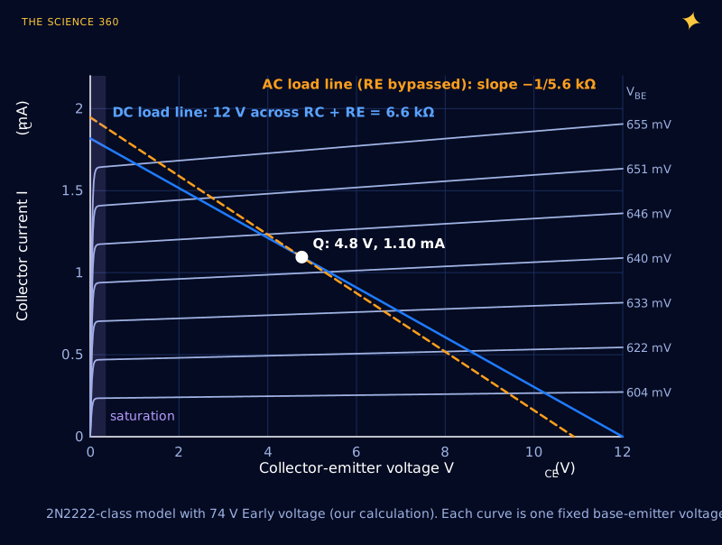
Three things are visible at a glance. The curves are nearly flat, so the transistor behaves like a current source controlled by VBE; their slight upward tilt is the Early effect that limits intrinsic gain. Adjacent curves, 0.25 mA apart, are separated by only 5 to 18 mV of VBE, which is the transconductance seen from the other side. And the signal actually moves along the orange AC load line, whose slope is set by RC alone. Along it, the collector can swing from 4.8 V down to roughly 0.3 V (about 4.5 V of room) before saturation, and up by before the transistor cuts off. The smaller of those, about 4.5 V peak, is the most this stage can deliver, and the next section shows why you rarely get near it.
Connect a load and the AC load line steepens further. A 10 kΩ load in parallel with RC and ro leaves 3.4 kΩ, and the gain falls from −220 to −145. This is why a high-gain stage is usually followed by a buffer.
Why does a transistor amplifier distort?
The gain formula assumed the curve in Figure 2 is a straight line over the input swing. It is an exponential, and the error grows fast. For an input of peak amplitude vp, the collector current is , and expanding that exponential gives a second harmonic whose size relative to the fundamental is about :
Our FFT of the exact waveform at 10 mV peak: 9.7%.
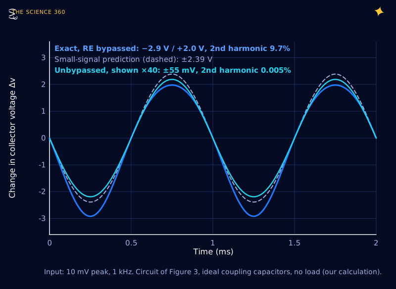
So the high-gain version of this amplifier is only a good amplifier for inputs of a millivolt or so. That suits a dynamic microphone or a magnetic pickup, and it is useless for a 1 V line signal, which would slam the collector from rail to rail.
The usual fix is emitter degeneration: leave some or all of RE unbypassed. The input voltage now has to drive the junction and raise the emitter, so most of vin appears across RE rather than across the junction, and the junction sees only a fraction of a millivolt:
Junction share of vin: , so 10 mV in puts only 0.23 mV across VBE.
Result (Figure 5, green): ±55 mV out, second harmonic 0.005%.
You trade a factor of 44 in gain for a factor of almost 2,000 in distortion. Negative feedback in general works this way, and the gain now depends on a resistor ratio instead of on temperature and VT. A compromise is to split RE into a small unbypassed part and a bypassed part, setting the gain anywhere between the two extremes.
So is the “small current controls a big current” explanation wrong?
It is incomplete in a way that misleads. Three corrections, in order of how often they trip people up.
First, energy. The bigger output is paid for by the supply, every joule of it, and an amplifier with no supply amplifies nothing. Feed a sine wave into the base of an unpowered transistor and the "output" is at best a diode-clipped copy of the input.
Second, what controls what. Base current and collector current are both consequences of VBE. Treating β as the gain mechanism suggests that a high-β transistor gives a high-gain amplifier, and it does not: at a fixed collector current, gain is for any bipolar transistor. β only buys a higher input resistance.
Third, linearity. A transistor is a strongly nonlinear device that we coax into acting linearly by biasing it, keeping signals small, and wrapping it in feedback. The same exponential that gives 59 mV per decade gives 10% distortion at 10 mV. The same transistor driven hard is a switch, with all the gain-independence that implies, which is the subject of our base resistor calculation post. Noise-cancelling headphones, which have to amplify microphone signals cleanly before they can subtract anything, rely on exactly these trade-offs; see how noise-cancelling headphones work.
One practical footnote: a stage with a gain of 200 will happily amplify ripple and noise on its own supply rail too. Local decoupling at the collector resistor's supply end matters, for the reasons in why 100 nF is the standard decoupling capacitor.
FAQ
Does a transistor create energy when it amplifies?
No. All the output power comes from the DC power supply. The transistor acts as a valve: a small input signal changes how much supply current flows through the load. In a typical small common-emitter stage the supply delivers about 16 mW and less than 0.03% of it leaves as signal.
Does a transistor amplify current or voltage?
Either, depending on the circuit. Physically, a bipolar transistor's collector current is set exponentially by the base-emitter voltage, and the base current is a small by-product. A collector resistor converts the current change into a voltage change, so a common-emitter stage gives both current gain and voltage gain.
What is the gain of a common-emitter amplifier?
With the emitter bypassed, the voltage gain is about , where gm equals the collector current divided by the thermal voltage of 25.7 mV at room temperature. That simplifies to the DC voltage across RC divided by 25.7 mV. With 6 V across RC the gain is about 230. Current gain β does not appear in the formula.
Why is a transistor amplifier output inverted?
In a common-emitter stage the output is taken at the collector, below the collector resistor. When the input rises, collector current rises, the voltage drop across the resistor grows, and the collector voltage falls. So the output moves opposite to the input, a 180° phase shift.
Why does a transistor amplifier need biasing?
A silicon transistor conducts almost nothing until the base-emitter voltage reaches about 0.6 V, and the exponential relation is only close to straight over a few millivolts. Biasing sets a steady operating current and collector voltage so that the signal rides on a nearly linear part of the curve with room to swing both ways.
Related on The Science 360
Sources
- NIST CODATA, Boltzmann constant (exact): physics.nist.gov/cgi-bin/cuu/Value?k; elementary charge (exact): physics.nist.gov/cgi-bin/cuu/Value?e
- MIT OpenCourseWare 6.012 Microelectronic Devices and Circuits, Spring 2009, Recitation 19 (, small-signal model, loaded transconductance gain): ocw.mit.edu 6.012 rec19 PDF
- Walla Walla University ENGR 356 Lab 8 (, compare measured gain with ): gab.wallawalla.edu lab8 PDF
- onsemi, BC546/BC547/BC548 datasheet, Rev. 8 (hFE 110 to 800 at 2 mA): onsemi.com/pdf/datasheet/bc546-d.pdf
- onsemi, P2N2222A datasheet, Rev. 7 (hFE ranges, no Early voltage listed): onsemi.com/pdf/datasheet/p2n2222a-d.pdf
- Typical page-one explanation ("small current controls a larger current"): All About Circuits forum, "How does a transistor amplify voltage?": forum.allaboutcircuits.com
Method note: all numbers for the Figure 3 circuit, Figures 1, 2, 4 and 5 and the β sweep are our own calculations in Python from the Shockley law, a simplified Gummel-Poon model and the formulas shown, at 25 °C with ideal capacitors.
Header image: NASA (image jsc2025e015685), regraded for this article.