3.3V to 5V Level Shifter: When You Need One and Why
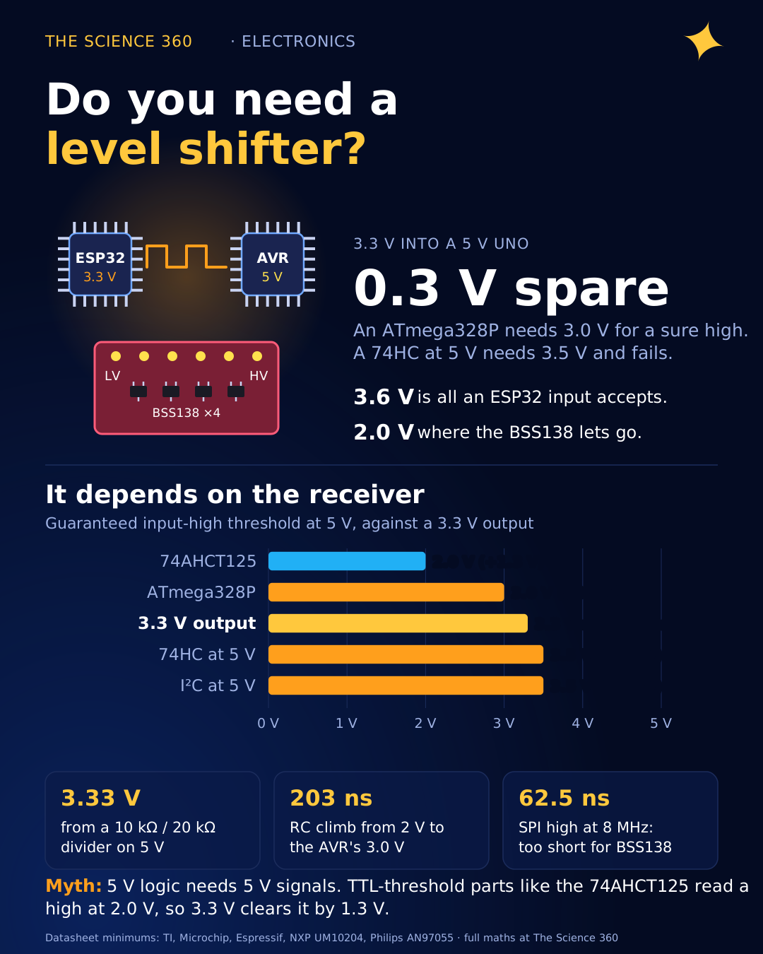
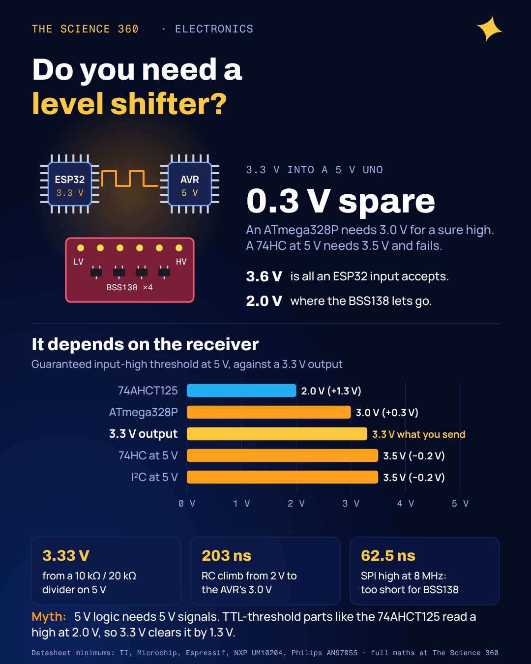
Connect a 3.3 V ESP32 output to a 5 V Arduino Uno input and it will almost certainly work on your bench. The ATmega328P needs 3.0 V to guarantee a high, and you are giving it 3.3 V: a margin of 0.3 V, about one tenth of what most logic designers would want. Plug the same ESP32 into a 74HC chip running from 5 V and it may not work at all, because that input wants 3.5 V. The question "do I need a level shifter?" has a different answer for every receiver, and that is the part most product pages and forum threads skip.
Page one for this search is mostly modules for sale and forum threads recommending them. They rarely say which direction needs shifting, how the BSS138 board works, or why its 10 kΩ pull-ups are too slow for fast I2C. We cover all three below.
Which direction actually needs a level shifter?
5 V into 3.3 V is about survival. Espressif's ESP32 datasheet gives the high-level input voltage as minimum and maximum. At 3.3 V supply that ceiling is 3.6 V. The RP2040 datasheet lists an absolute maximum "Voltage at IO" of , so 3.8 V. Feed either one 5 V and you are forward-biasing the input protection diodes into the 3.3 V rail, which is exactly what those ratings forbid.
3.3 V into 5 V is about thresholds. Nothing is overstressed; the question is whether the receiver sees a high. Figure 1 shows four common 5 V receivers.
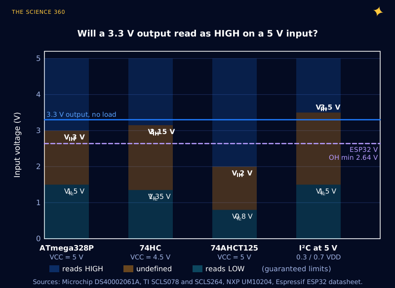
Receiver at 5 V, VIH(min) → margin for a 3.3 V output (unloaded):
74AHCT125 (TTL levels):
ATmega328P:
ATmega328P at VCC = 5.5 V:
74HC: 3.15 V at VCC = 4.5 V and 4.2 V at 6 V, both :
The ATmega328P result needs one more number. The ESP32 datasheet guarantees of only , and that is below the 3.0 V the AVR needs. In practice a lightly loaded CMOS output sits within millivolts of its rail, and the ATmega's typical switching threshold, from the characteristic curve in Microchip's datasheet, is about 2.6 V at 5 V supply. So a direct 3.3 V to Uno connection works in practice, but no datasheet guarantees it.
The misconception: “5 V logic needs 5 V signals”
Page one's usual advice, "use a level shifter whenever you mix 3.3 V and 5 V", treats 5 V logic as one thing. It is two. CMOS families like 74HC switch near half the supply and need about for a guaranteed high. TTL-compatible families (74HCT, 74AHCT and the original bipolar TTL they imitate) switch at fixed levels: TI's SN74AHCT125 datasheet specifies VIH = 2 V and VIL = 0.8 V across its whole 4.5 to 5.5 V supply range.
So a 74AHCT125 on a 5 V supply is the cleanest one-way 3.3 V to 5 V shifter: its input reads 3.3 V with 1.3 V to spare and its push-pull output keeps edges fast, ideal for clocks, chip selects and LED strip data. The mirror-image part for going down is TI's SN74LVC125A on 3.3 V, whose "inputs accept voltages to 5.5V".
How does the BSS138 bidirectional level shifter work?
The red and blue breakout boards use a circuit from Philips application note AN97055 (Herman Schutte, 1997): one N-channel MOSFET and two pull-ups per channel (Figure 2), gate to the low supply, source to the low-voltage line, drain to the high-voltage line.
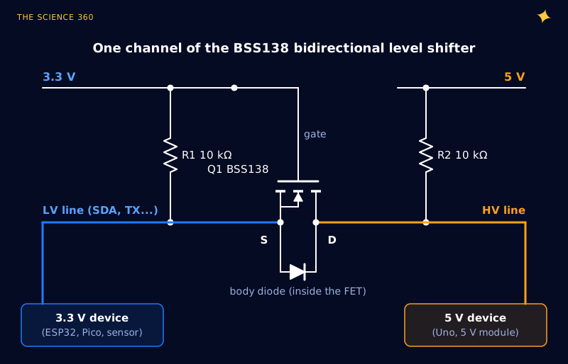
AN97055 walks through three states. I paraphrase them with BSS138 numbers from the onsemi datasheet (VGS(th) 0.8 V min, 1.3 V typical, 1.5 V max):
Idle. Nobody pulls the line down. The low side sits at 3.3 V, so and the FET is off. The high side floats up to 5 V on its own pull-up. Both lines read high, each at its own voltage.
The 3.3 V device pulls low. The source drops toward 0 V while the gate stays at 3.3 V. VGS climbs to 3.3 V, well above threshold, and the FET connects the two lines. The 5 V side is pulled low through the channel.
The 5 V device pulls low. Now the drain falls, and the body diode conducts from the 3.3 V side into it, pulling the source down. Once the source is about 2 V below the gate, the FET turns on and pulls the low side the rest of the way. Both lines end up low together.
FET turn-off point on a rising edge:
Typical; 1.8 to 2.5 V across the datasheet's 0.8 to 1.5 V range.
AN97055's measured waveforms: "At about 2 Volt on the rising edge, the MOS-FET is switched off and each section rises smoothly with its own curve."
That 2 V knee is the key to the circuit's speed. Below it the two sides move together. Above it the 5 V side is on its own, and nothing but its pull-up resistor drags it up to 5 V.
Why is the BSS138 level shifter slow?
Every rising edge on the 5 V side ends as an RC charge through the pull-up, even when the 3.3 V side is driven by a fast push-pull output. Figure 3 shows our simulation of both cases with the values on the popular modules: 10 kΩ on each side, which Adafruit's product page confirms for its four-channel BSS138 board, and an assumed 50 pF per side for a breadboard, wires and a couple of inputs.
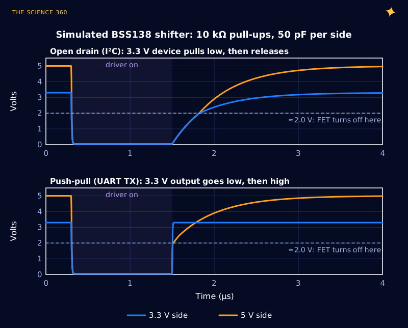
For the push-pull case the rise above the knee is a plain exponential, which is the same arithmetic as in why the RC time constant is 63%:
Time from 2.0 V to a 5 V input threshold VT:
To ATmega328P VIH = 3.0 V:
To 74HC VIH ≈ 3.5 V:
To 90% (4.5 V):
A 115,200 baud UART bit lasts , so a 0.2 µs delay is 2% of a bit and harmless (the timing budget for that is covered in UART baud rate error tolerance). An Uno's fastest SPI clock is 8 MHz, half of its 16 MHz system clock, giving a high phase of 62.5 ns: the 5 V side would not even reach the AVR threshold before the clock falls again. That is why Adafruit's own page limits its BSS138 board to "slow <2MHz SPI" and points to the TXB0108 or 74LVC245 for anything fast.
Is a BSS138 level shifter fast enough for 400 kHz I2C?
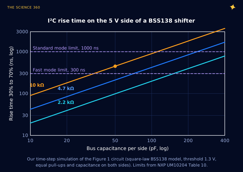
The I2C specification (NXP UM10204, Table 10) caps the rise time, measured from 30% to 70% of VDD, at 1,000 ns for Standard mode (100 kHz) and 300 ns for Fast mode (400 kHz). For a plain pull-up it gives the formula . Through the shifter the 5 V side behaves a little worse than that, because its edge has to wait for the 3.3 V side to bring both lines up to the 2 V knee. Figure 4 plots our simulated rise time for three pull-up values.
Plain pull-up, 10 kΩ, 50 pF:
Through the shifter (simulation): 450 ns on the 5 V side, 332 ns on the 3.3 V side.
Fast-mode limit 300 ns → largest bus capacitance per side (simulation): 10 kΩ: about 33 pF; 4.7 kΩ: about 70 pF; 2.2 kΩ: about 150 pF.
Standard-mode limit 1,000 ns → 10 kΩ: about 110 pF.
So the standard red board runs 100 kHz I2C over almost anything, and runs 400 kHz only on a short, tidy bus. Many sensor breakouts carry their own 10 kΩ pull-ups, which sit in parallel with the shifter's and halve the effective resistance; count them before adding more. Going lower than 2.2 kΩ is limited by the sink current the devices can handle: UM10204 specifies VOL at 3 mA sink current for Standard and Fast mode, which works out to a minimum of on the 5 V side. The theory behind choosing that resistor is in how to choose a pull-up resistor value.
When are two resistors enough?
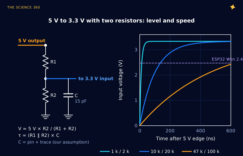
For a one-way 5 V to 3.3 V signal, such as a 5 V module's UART TX into an ESP32's RX, a voltage divider is a perfectly good shifter. Unlike a divider used as a power supply, it only has to drive a CMOS input that draws microamps. Figure 5 shows what the resistor values do to its edges.
Level:
Check the high side: if the 5 V rail is really 5.5 V, , just over ESP32's 3.6 V VIH(max); 1.8 kΩ over 3.3 kΩ gives 3.56 V instead.
Speed, 10 kΩ/20 kΩ:
Time to ESP32 :
Static current when high:
With 1 kΩ/2 kΩ: 1.7 mA, .
At 136 ns the 10 kΩ/20 kΩ pair is fine for any UART speed an Arduino uses and for slow SPI. For a few megahertz, drop to 1 kΩ/2 kΩ and accept 1.7 mA while the line is high, which the 5 V output can supply easily (see how much current an Arduino pin can supply). Do not go the other way to 47 kΩ/100 kΩ to save power: the edge then takes over 600 ns to cross the threshold, and a slow edge on a non-Schmitt input invites double-clocking.
A divider cannot shift up or work on a bidirectional line like I2C SDA. A lone series resistor that leans on the clamp diodes is a common hack, but it pushes current into the 3.3 V rail and neither Espressif nor Raspberry Pi rates a pin for it.
What about 5 V-tolerant pins?
Some 3.3 V chips take 5 V inputs directly; AN97055 calls them "5 Volt tolerant I/O's". Where a datasheet says so explicitly for a pin, connect 5 V logic with no shifter.
Be careful with names, though. The RP2040 has pins labelled "FT", for Fault Tolerant, and the datasheet defines that narrowly: "very little current flows into the pin whilst it is below 3.63V and IOVDD is 0V." That protects an unpowered chip from a powered 3.3 V bus. It does not make the pin 5 V tolerant.
Which level shifter should you use?
Match the tool to the signal rather than buying the same red board for everything:
| Signal | Direction | Best choice | Why |
|---|---|---|---|
| UART TX, 5 V → 3.3 V | Down | 10 kΩ / 20 kΩ divider | Two parts, 136 ns edge, fine to 1 Mbaud |
| UART TX, 3.3 V → 5 V AVR | Up | Direct, or 74AHCT125 | 3.0 V threshold; direct works but with 0.3 V margin |
| SPI clock and data, LED strip data | Up | 74AHCT125 at 5 V | TTL input, push-pull output, fast edges |
| Fast 5 V signals into 3.3 V | Down | 74LVC125A at 3.3 V | Inputs accept 5.5 V, push-pull 3.3 V out |
| I2C, 1-Wire, any open-drain line | Both | BSS138 shifter | Bidirectional without a direction pin; size pull-ups to Figure 4 |
One last case: if all you need is to switch a 5 V load from a 3.3 V pin, that is not level shifting at all. Use a logic-level MOSFET (see choosing a MOSFET gate resistor value) or a transistor sized as in how to calculate a transistor base resistor.
FAQ
Do I need a level shifter between 3.3 V and 5 V?
Going 5 V to 3.3 V, almost always: 5 V exceeds the input rating of ESP32 and RP2040 pins. Going 3.3 V to 5 V, it depends on the receiver. A 74AHCT or 74HCT input needs only 2.0 V and reads 3.3 V easily. An ATmega328P needs 3.0 V, so 3.3 V works with little margin. A 74HC or 5 V I2C input needs 3.5 V and will not reliably see 3.3 V as high.
How does a BSS138 level shifter work?
The MOSFET gate is tied to 3.3 V, its source to the 3.3 V line and its drain to the 5 V line, with a pull-up on each side. When both sides are idle the FET is off and each side sits at its own supply. If the 3.3 V side is pulled low, the gate-source voltage rises above threshold and the FET pulls the 5 V side low. If the 5 V side is pulled low, the body diode drags the 3.3 V side down until the FET turns on and finishes the job.
Can a BSS138 level shifter handle 400 kHz I2C?
Only with low capacitance or stronger pull-ups. With the common 10 kΩ pull-ups, our simulation gives a 30 to 70% rise time on the 5 V side of about 450 ns at 50 pF per side, beyond the 300 ns Fast-mode limit. 10 kΩ meets 300 ns only below about 33 pF per side; 4.7 kΩ reaches about 70 pF and 2.2 kΩ about 150 pF.
Can I use a voltage divider to go from 5 V to 3.3 V?
Yes, for one-way signals such as a 5 V UART TX into a 3.3 V RX. 10 kΩ over 20 kΩ gives 3.33 V and, with about 15 pF of input capacitance, a 100 ns time constant, fine for UART but too slow for fast SPI. Use 1 kΩ over 2 kΩ for faster edges, at the cost of 1.7 mA when the line is high.
Are ESP32 and Raspberry Pi Pico pins 5 V tolerant?
Not according to their datasheets. The ESP32 datasheet gives a maximum input high voltage of VDD plus 0.3 V, about 3.6 V. The RP2040 absolute maximum is IOVDD plus 0.5 V, and its fault-tolerant pins are only rated to 3.63 V while unpowered.
Related on The Science 360
Sources
- Herman Schutte, Philips Semiconductors, AN97055 "Bi-directional level shifter for I²C-bus and other systems" (1997): three operating states, 2 V switch-off point, MOSFET requirements, 5 V tolerant I/O: cdn-shop.adafruit.com/datasheets/an97055.pdf
- onsemi, BSS138 N-channel logic level MOSFET datasheet (VGS(th) 0.8/1.3/1.5 V, RDS(on) 1.0 Ω typical at 4.5 V, Ciss 27 pF): onsemi.com BSS138 datasheet
- NXP, UM10204 I²C-bus specification and user manual, Rev. 7.0 (rise time limits 1000/300 ns, , VIH 0.7 VDD, VOL at 3 mA): nxp.com UM10204
- Texas Instruments, SN74AHCT125 datasheet SCLS264R (VIH 2 V, VIL 0.8 V at VCC 4.5 to 5.5 V): ti.com SN74AHCT125
- Texas Instruments, SN74HC04 datasheet SCLS078H (VIH 3.15 V at 4.5 V, 4.2 V at 6 V): ti.com SN74HC04
- Texas Instruments, SN74LVC125A datasheet SCAS290T ("Inputs accept voltages to 5.5V"): ti.com SN74LVC125A
- Microchip, ATmega48A/PA/88A/PA/168A/PA/328/P datasheet DS40002061A (VIH 0.6 VCC, VIL 0.3 VCC, typical input threshold curve Fig. 31-356): microchip.com DS40002061A
- Espressif, ESP32 Series Datasheet (VIH to , VOH ): espressif.com ESP32 datasheet
- Raspberry Pi, RP2040 Datasheet, section 5.5.3 (VPIN max , definition of Fault Tolerant pins): datasheets.raspberrypi.com RP2040
- Adafruit, 4-channel I2C-safe bi-directional logic level converter, BSS138, product 757 (10 kΩ pull-ups, "slow <2MHz SPI"): adafruit.com/product/757
Method note: Figures 3 and 4 are time-step simulations we wrote of the AN97055 circuit with a square-law BSS138 model; Figure 5 is the analytic RC response of a divider with an assumed 15 pF load. Threshold values in Figure 1 are datasheet minimums and maximums; the 3.5 V value for 74HC at 5 V is our interpolation of TI's 4.5 V and 6 V figures.
Header image: NASA/ESA (Thomas Pesquet) (image iss050e011416), regraded for this article.