How do logic gates work?
A logic gate takes one or two inputs that are each either 0 (LOW) or 1 (HIGH) and produces one output by a fixed rule. AND gives 1 only when both inputs are 1, OR gives 1 when at least one is, NOT flips its input, and XOR gives 1 when the inputs differ. NAND, NOR and XNOR are the same three rules with the output inverted. That is the whole list. Every digital circuit, from a doorbell timer to a phone processor, is these seven rules wired together.
The simulator shows the rule three ways at once: wires turn green when they are HIGH, the output lamp lights, and the truth table highlights the row your inputs select. Each gate also shows the real 14-pin chip it comes in. A 74HC00 holds 4 NAND gates and switches in about 9 ns at 4.5 V. To connect gates to a microcontroller you also need sensible input levels and pull-up resistors, which the pull-up resistor guide and the 3.3 V to 5 V level shifter post cover.
Key results from the simulation
- Output columns (inputs 00, 01, 10, 11): AND 0001, OR 0111, NAND 1110, NOR 1000, XOR 0110, XNOR 1001. NOT turns 0 into 1 and 1 into 0.
- Rows = 2 to the power of the inputs: two inputs give 4 rows, three inputs give 8. That is why a full adder table is twice as long as a half adder table.
- NAND builds everything: NOT takes 1 NAND, AND 2, OR 3, NOR 4, XOR 4 and XNOR 5. The builder preset shows two NANDs making an AND.
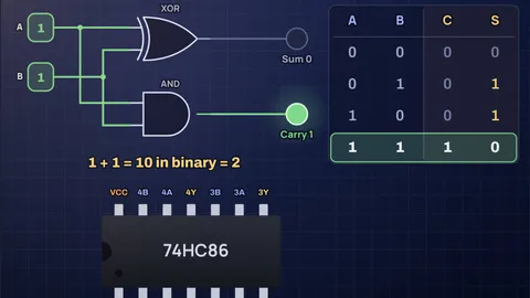
- Adding with gates: a half adder gives 1 + 1 = 10 in binary. A full adder adds three bits, so 1 + 1 + 1 = 11, which is 3.
- Speed: at about 9 ns per 74HC gate and two gate delays per bit on the carry path, an 8-bit ripple adder settles in about 144 ns and a 32-bit one in about 576 ns.
Six gates and circuits to try
Each section explains one setup, gives the numbers the simulation shows and has a button that loads it. Tap the input keys on the stage afterwards to walk through the other rows.
AND gate: both inputs must be 1
Two inputs, one outputThe AND gate is a series connection in disguise: think of two switches in a line with a lamp. Current only reaches the lamp if both are closed. Its truth table output column reads 0, 0, 0, 1, so three of the four rows are 0. The Boolean expression is Y = A · B, where the dot means AND.
On a breadboard the gate comes as a 74HC08 with 4 independent gates, power on pin 14 and ground on pin 7. A typical use is an enable signal: the clock only passes through when the enable line is HIGH. On a microcontroller the same thing is the && operator in an if statement.
XOR gate: 1 when the inputs differ
Exclusive ORXOR is OR with the "both" case removed. Its output column is 0, 1, 1, 0. Another way to read it: B decides whether A passes through unchanged (B = 0) or inverted (B = 1). That makes XOR a controllable inverter, and it is why it shows up in parity checkers, error detecting codes, simple ciphers and the sum bit of every adder.
The classic real-world XOR is a staircase light with a switch at the top and the bottom. Flipping either switch changes the state of the lamp, whatever the other switch is doing. The chip is the 74HC86, and building one from NAND gates takes 4 of them.
NAND gate: the one gate that can build the rest
NOT ANDNAND is AND followed by NOT, so its output column is the AND column flipped: 1, 1, 1, 0. The small circle on the output of the symbol is the inversion bubble. The same bubble turns OR into NOR and XOR into XNOR.
NAND matters because it is functionally complete: any truth table can be built from NAND gates alone. In CMOS a NAND also needs fewer transistors than an AND (four against six), so chip designers reach for it first. The quad NAND is part number 7400 itself, the first in the family.
Two NANDs make an AND
Gate builderThe builder chains two gates: the first combines A and B into X, the second combines X with C. Load this preset and C is held at 1. A NAND with one input fixed at 1 just inverts the other input, so the second gate undoes the inversion of the first and Y follows A AND B.
Walk through the table: in every row where C = 1, Y matches the AND column 0001. Swap the second gate for an OR or an XOR in the drop-down and you have built a three-input function from two parts, which is exactly how logic is designed in practice.
Half adder: how a computer adds 1 + 1
XOR plus ANDAdding two single bits has four cases: 0 + 0 = 0, 0 + 1 = 1, 1 + 0 = 1 and 1 + 1 = 2, which is 10 in binary. The right-hand digit (the sum) is the XOR column 0110 and the left-hand digit (the carry) is the AND column 0001. So one XOR and one AND add two bits.
It is called half because it has no input for a carry coming from the previous column. That is enough for the lowest bit of a sum and nothing more.
Full adder: the cell inside every CPU adder
Two half adders and an ORA full adder adds A, B and a carry in. The first XOR makes P = A XOR B, the second XOR adds the carry to give the sum, and either AND gate firing produces a carry out through the OR. With all three inputs at 1 the answer is 11 in binary, which is 3.
Chain eight of these, carry out to carry in, and you have an 8-bit adder. The carry has to ripple through two gates per bit, so with 74HC gates at about 9 ns each the worst case is about 144 ns. Processors use carry-lookahead tricks to avoid that wait.
All seven gates at a glance
| Gate | Expression | Output for 00, 01, 10, 11 | IEC label | 7400 chip | NANDs to build |
|---|---|---|---|---|---|
| AND | Y = A · B | 0, 0, 0, 1 | & | 74HC08 (quad 2-input AND) | 2 |
| OR | Y = A + B | 0, 1, 1, 1 | ≥1 | 74HC32 (quad 2-input OR) | 3 |
| NOT | Y = NOT(A) | A = 0 gives 1, A = 1 gives 0 | 1 with bubble | 74HC04 (hex inverter) | 1 |
| NAND | Y = NOT(A · B) | 1, 1, 1, 0 | & with bubble | 74HC00 (quad 2-input NAND) | 1 |
| NOR | Y = NOT(A + B) | 1, 0, 0, 0 | ≥1 with bubble | 74HC02 (quad 2-input NOR) | 4 |
| XOR | Y = A ⊕ B | 0, 1, 1, 0 | =1 | 74HC86 (quad 2-input XOR) | 4 |
| XNOR | Y = NOT(A ⊕ B) | 1, 0, 0, 1 | =1 with bubble | 74HC7266 (quad 2-input XNOR) | 5 |
Chip numbers are the 74HC CMOS versions, which run from 2 V to 6 V. The same functions exist as 74LS (TTL, 5 V), 74HCT (TTL input levels) and 74LVC (down to 1.65 V). The NAND counts are the minimum two-input NAND gates needed for each function.
How the simulation works
Each gate is one line of logic in the code: AND is a & b, OR is a | b, XOR is a ^ b, and the inverted gates subtract that result from 1. The truth table is generated by running the same function over every input combination in binary counting order, so the highlighted row number is just the inputs read as a binary number plus one.
The half adder computes the sum with XOR and the carry with AND. The full adder is built as it is on a real board: P = A XOR B, sum = P XOR Cin, carry out = (A AND B) OR (P AND Cin). The builder computes X = G1(A, B) and then Y = G2(X, C). The drawn wires are coloured by the level the code computes for that node, so a mistake in the wiring would show up as a mismatch between the lamp and the table.
Symbols follow the two standards you will meet: the distinctive shapes of ANSI/IEEE Std 91 (used in most US and Indian textbooks) and the rectangular boxes of IEC 60617 (used in European schematics), where & means AND, ≥1 means OR, =1 means XOR and 1 means a buffer. Chip timing uses the TI SN74HC00 datasheet: 9 ns typical and 18 ns maximum at 4.5 V and 25 °C.
What the model leaves out
- Real voltages: the simulation uses ideal 0 and 1. A real 74HC gate at 4.5 V reads anything above 3.15 V as HIGH and anything below 1.35 V as LOW. Between the two the output is undefined and the chip draws extra current.
- Timing: outputs change instantly here. Real gates take nanoseconds, and different paths take different times, which can make brief false pulses called glitches.
- Floating inputs: an unconnected CMOS input is neither 0 nor 1 and can oscillate. On a breadboard every unused input must be tied to VCC or ground, often through a pull-up resistor.
- Fan-out and loading: one output can drive many inputs, but only a few milliamps into an LED. The simulator does not model output current.
- Sequential logic: gates with feedback make latches and flip-flops that remember. This simulator covers combinational logic only, where the output depends on the present inputs alone.
Common misconceptions
“XOR and OR are the same except for one row, so it does not matter which you use.” That one row is the whole point. OR is 1 when both inputs are 1, XOR is 0. Use OR in an adder and 1 + 1 comes out as 1.
“A NAND gate is an AND gate and a NOT gate inside the chip.” In CMOS it is the other way round. The NAND is the natural, cheaper structure (four transistors) and an AND gate is built as a NAND followed by an inverter (six transistors).
“0 means 0 V and 1 means 5 V exactly.” Logic levels are bands, not exact voltages. That is why a 3.3 V output can sometimes drive a 5 V input and sometimes cannot, see the level shifter post.
Frequently asked questions
What are the 7 basic logic gates?
AND, OR, NOT, NAND, NOR, XOR and XNOR. AND, OR and NOT are the basic three. NAND, NOR and XNOR are AND, OR and XOR with the output inverted, and XOR gives 1 when its two inputs are different.
Why are NAND and NOR called universal gates?
Because any logic function can be built from NAND gates alone, or from NOR gates alone. With NAND, a NOT takes 1 gate, AND takes 2, OR takes 3 and XOR takes 4. Manufacturers like this because one gate design can be repeated across the chip.
How many rows does a truth table have?
Two to the power of the number of inputs. A two-input gate has 4 rows, a three-input circuit such as a full adder has 8, and a four-input circuit has 16.
What is the difference between a half adder and a full adder?
A half adder adds two bits and gives a sum and a carry, using one XOR and one AND. A full adder also accepts a carry in from the previous bit, using two XORs, two ANDs and one OR, so full adders can be chained to add numbers of any length. 1 + 1 + 1 gives 11 in binary.
Which IC has AND, OR or NAND gates?
In the 7400 family: 7400 is quad NAND, 7402 quad NOR, 7404 hex inverter (NOT), 7408 quad AND, 7432 quad OR and 7486 quad XOR. The 74HC versions run from 2 V to 6 V. Note that the 7402 has a different pinout, with each output on the first pin of its group.
What do the ANSI and IEC logic symbols mean?
ANSI/IEEE symbols use a distinct shape per gate, such as the D shape for AND and the curved shield for OR. IEC 60617 symbols are all rectangles with a label inside: & for AND, ≥1 for OR, =1 for XOR and 1 for a buffer, plus a small circle on the output for an inverted gate.
Keep learning
Logic Gate Symbols and Truth Tables (Printable Chart)
All 7 logic gates in one chart: ANSI and IEC symbols, Boolean expressions, truth tables, 7400 series chip numbers and the half adder, with worked examples.

3.3V to 5V Level Shifter: When You Need One and Why
When a 3.3 V output already reads as HIGH at 5 V, how the BSS138 shifter works, why its 10k pull-ups fail 400 kHz I2C, and when two resistors are enough.

How to Choose a Pull-Up Resistor Value (With I2C Math)
Pull-up resistors have a minimum set by sink current and a maximum set by rise time and leakage. Worked I2C example at 400 kHz, plus MCU internal pull-ups.
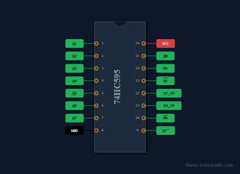
74HC595 Shift Register: Features, Working, and Control Using Arduino & Microcontrollers
The 74HC595 shift register is one of the most widely used ICs in electronics, embedded systems, and prototyping. Its ability to expand digital output