Logic Gate Symbols and Truth Tables (Printable Chart)
A 74HC00 chip costs less than a cup of tea, holds four NAND gates and switches each one in about 9 nanoseconds. Five chips from the same family (two XOR, two AND and one OR) are enough to add two 4-bit numbers. Every phone processor does the same job with billions of gates instead of sixteen, but the rules each gate follows have not changed since the 1960s, and there are only seven of them.
This post puts all seven on one page: the symbol you will see in an Indian or American textbook, the boxed symbol used in European schematics, the Boolean expression, the truth table and the chip that contains it. If you would rather press buttons than read, open the logic gate simulator: tap the inputs of any gate and watch the matching truth table row light up.
What do the logic gate symbols mean?
Two symbol sets are in common use, and a good engineer reads both.
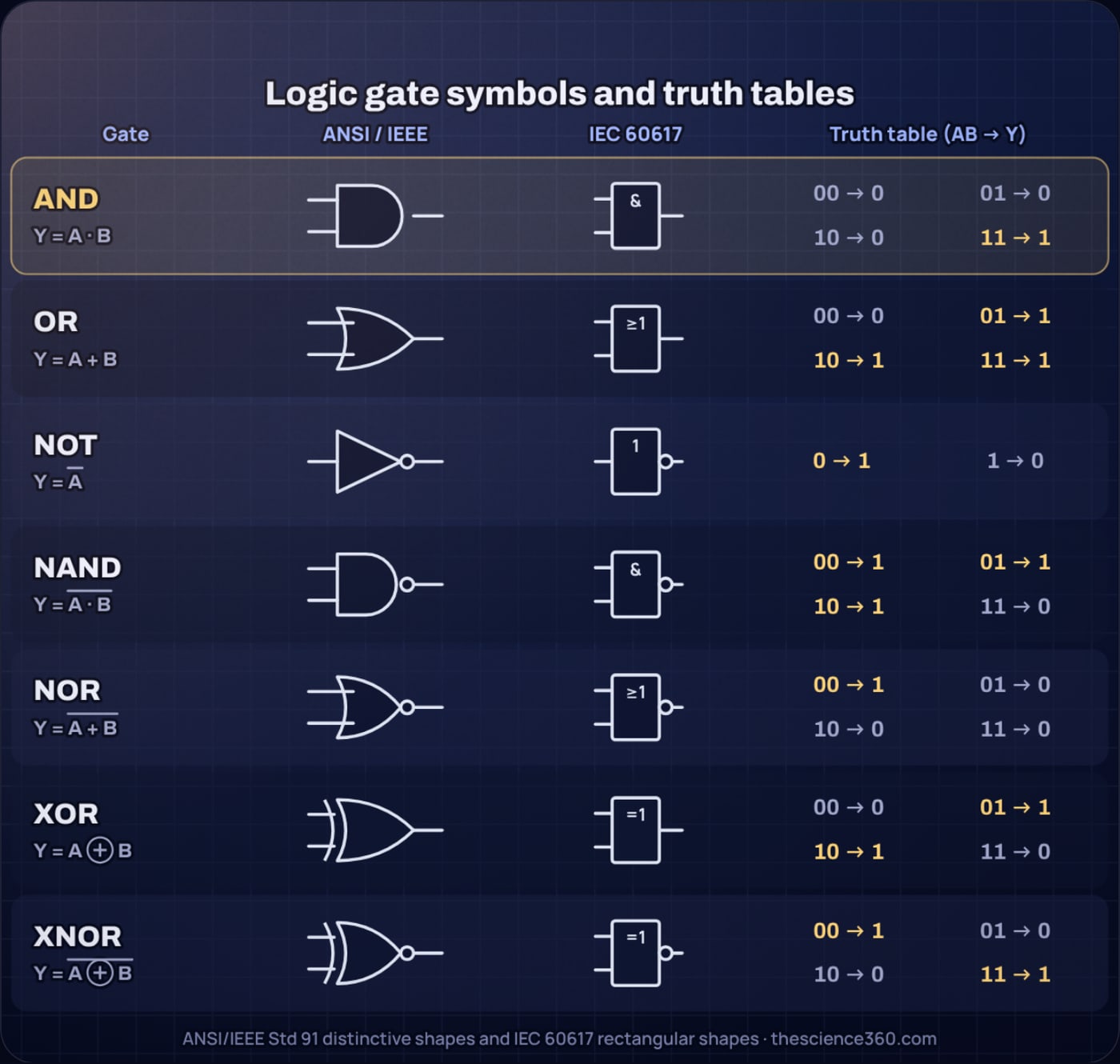
The distinctive shapes come from the US military standard MIL-STD-806 and were formalised as ANSI/IEEE Std 91. Each function has its own outline. AND is a D shape: a flat back and a round front. OR is a pointed shield with a curved back. NOT is a triangle. XOR is the OR shield with a second curved line behind the inputs. These are the shapes in CBSE and state board textbooks, in most Arduino tutorials and in nearly every datasheet from a US manufacturer.
The rectangular symbols come from IEC 60617-12, the international standard used across Europe and in a lot of industrial documentation. Every gate is the same box, and a short label inside says what it does. The label is a counting rule about how many inputs must be 1:
- & means all inputs must be 1 (AND).
- ≥1 means at least one input must be 1 (OR).
- =1 means exactly one input must be 1 (XOR).
- 1 on a single-input box means a buffer, and with an output circle it is an inverter (NOT).
Both systems share one mark: a small circle, the inversion bubble. Put it on the output and the whole truth table column flips. That is the only difference between AND and NAND, OR and NOR, XOR and XNOR, and between a buffer and a NOT gate. Once you see the bubble as an instruction to flip the column, you only need to learn three rules.
What are the truth tables for all 7 gates?
A truth table lists every possible input combination and the output for each. Write the rows by counting in binary (00, 01, 10, 11) so you never skip one. Here is the full set for two-input gates:
| A | B | AND | OR | NAND | NOR | XOR | XNOR |
|---|---|---|---|---|---|---|---|
| 0 | 0 | 0 | 0 | 1 | 1 | 0 | 1 |
| 0 | 1 | 0 | 1 | 1 | 0 | 1 | 0 |
| 1 | 0 | 0 | 1 | 1 | 0 | 1 | 0 |
| 1 | 1 | 1 | 1 | 0 | 0 | 0 | 1 |
NOT has one input, so its table has two rows: 0 gives 1 and 1 gives 0.
Read the columns as four-digit codes and the inverted pairs jump out. AND is 0001 and NAND is 1110. OR is 0111 and NOR is 1000. XOR is 0110 and XNOR is 1001. Each pair is the same code with every digit flipped.
How to write the Boolean expressions
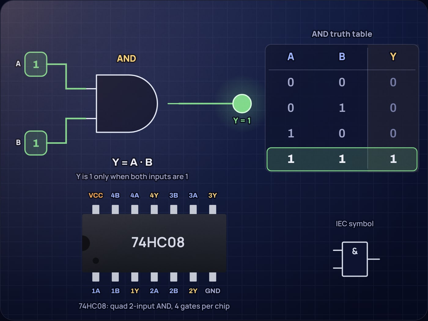
Boolean algebra gives each gate a short formula. AND is written as a product, , because multiplying 0s and 1s gives 1 only when both are 1. OR is written as a sum, , with the understanding that 1 + 1 is still 1. XOR has its own circled plus, . A bar over an expression inverts it:
A common slip is to read as . They are different gates. The first is NAND, which is 0 only for inputs 11. The second is NOR, which is 1 only for inputs 00. De Morgan's laws connect them: . Breaking the bar changes the operator.
How many rows does a truth table need?
Each input can be 0 or 1, and every extra input doubles the number of combinations. For n inputs:
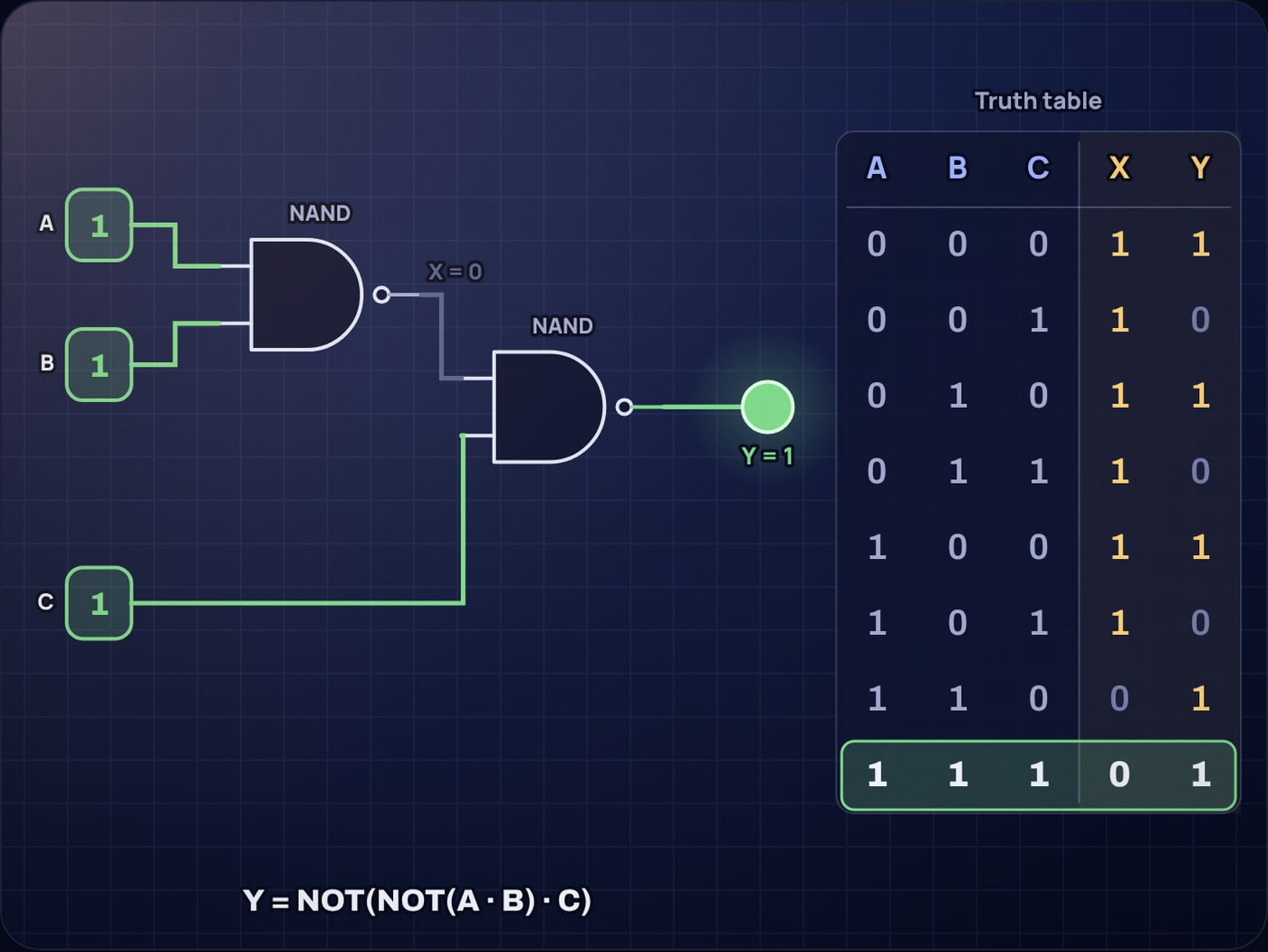
The simulator's builder mode does exactly this kind of chain: the first gate combines A and B into X, the second combines X with C, and the 8-row table updates as you change either gate.
Why is XOR different from OR?
The two tables differ in a single row, inputs 11. OR says 1, XOR says 0. That row matters more than it looks.
Think of a staircase light with a switch at the bottom and another at the top. Flipping either switch must change the light, whatever the other switch is doing. That is XOR: the output is 1 when the switches disagree. If the wiring followed OR, then once both switches were on, flipping one would leave the light on and you would be stuck.
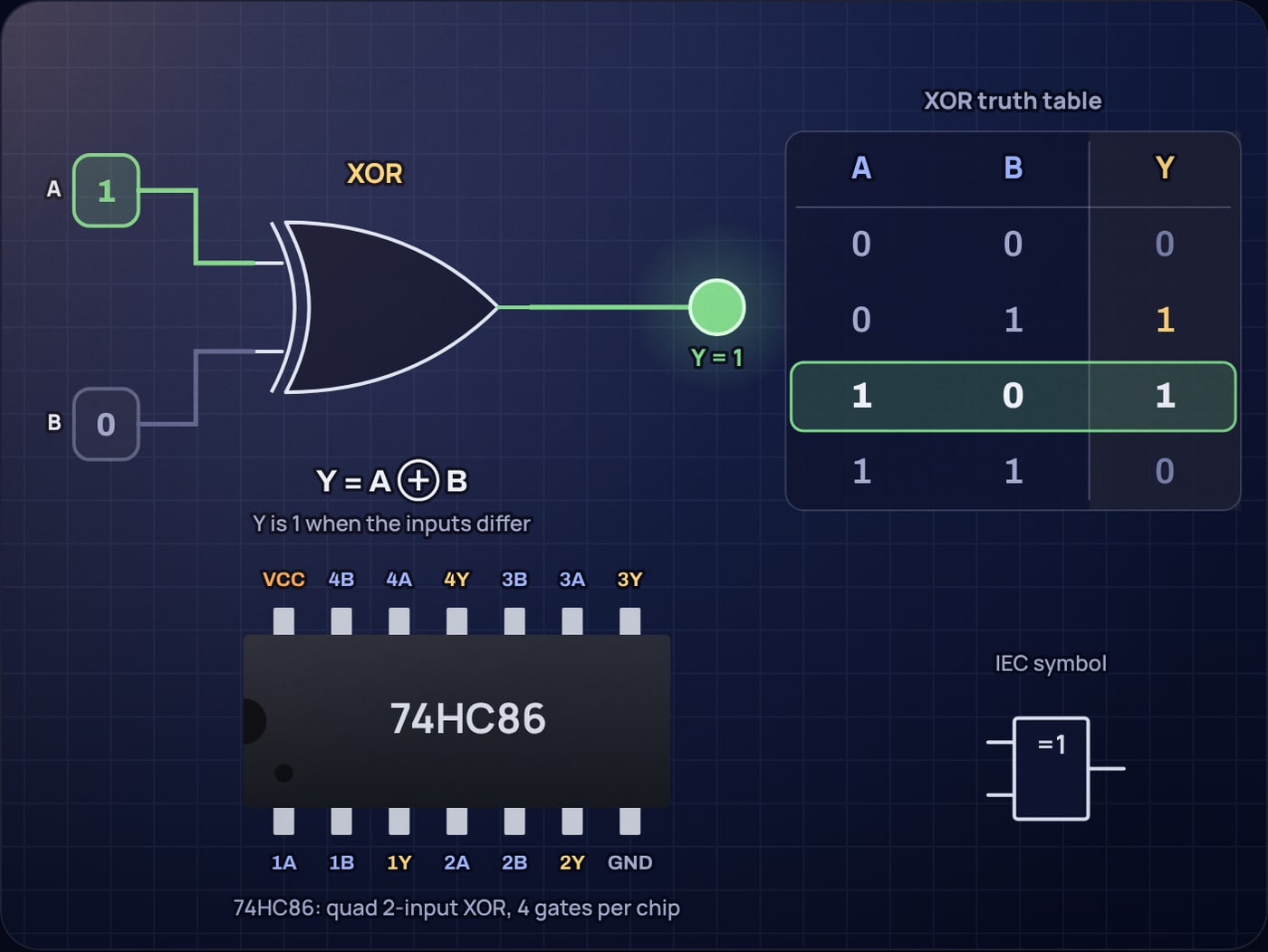
XOR is also a controllable inverter. With B = 0 the output equals A. With B = 1 the output is NOT A. That property puts XOR at the heart of parity checks, CRC error detection, simple stream ciphers and, most importantly, binary addition.
How do logic gates add numbers?
Add two single bits and there are four cases. 0 + 0 = 0, 0 + 1 = 1, 1 + 0 = 1 and 1 + 1 = 2, which is 10 in binary. Write the answer as two digits, a carry and a sum:
| A | B | Carry | Sum |
|---|---|---|---|
| 0 | 0 | 0 | 0 |
| 0 | 1 | 0 | 1 |
| 1 | 0 | 0 | 1 |
| 1 | 1 | 1 | 0 |
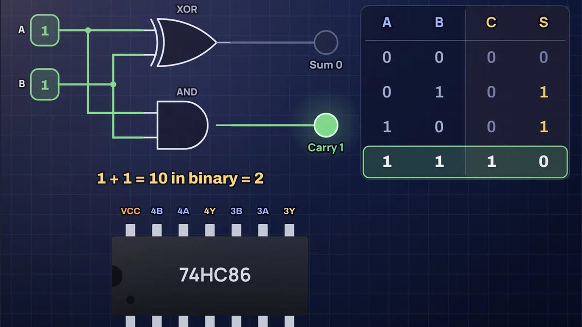
The sum column is 0110, the XOR column. The carry column is 0001, the AND column. So one XOR and one AND add two bits. That circuit is the half adder.
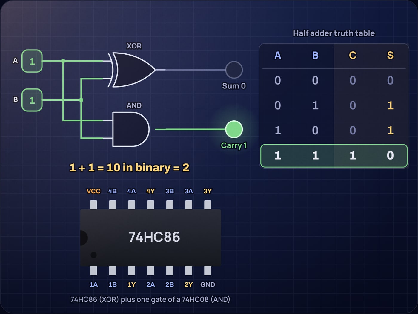
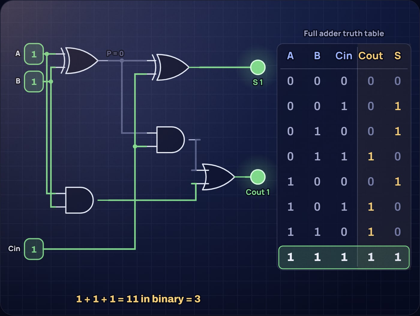
A half adder cannot accept a carry from the column to its right, so it can only handle the lowest bit. The full adder fixes that. It is two half adders and an OR gate: the first XOR makes , the second XOR adds the incoming carry, and the carry out is 1 if either AND gate fires.
Bit 0: 1 + 1 + 0 = 10, so sum 0, carry 1.
Bit 1: 0 + 1 + 1 = 10, so sum 0, carry 1.
Bit 2: 1 + 0 + 1 = 10, so sum 0, carry 1.
Bit 3: 0 + 0 + 1 = 01, so sum 1, carry 0.
Reading the sums from bit 3 down gives 1000, which is 8. Each line is one row of the full adder truth table, and you can check every one in the simulator by setting A, B and Cin.
How fast is a gate adder?
The carry has to pass through each full adder in turn, so a long adder waits for it. On the carry path each bit adds roughly two gate delays (an AND then the OR). The TI SN74HC00 datasheet gives a typical propagation delay of 9 ns at 4.5 V and a maximum of 18 ns at 25 °C.
Why are NAND and NOR called universal gates?
Any truth table you can write can be built from NAND gates alone. Tie both inputs of a NAND together and it becomes NOT. Follow a NAND with that NOT and you have AND. Put NOTs on the inputs of a NAND and De Morgan's law turns it into OR. The minimum counts using two-input NAND gates are:
| Gate | NAND gates needed |
|---|---|
| NOT | 1 |
| AND | 2 |
| OR | 3 |
| NOR | 4 |
| XOR | 4 |
| XNOR | 5 |
Here is the misconception worth correcting. Many students picture a NAND chip as an AND gate with a NOT bolted on. In CMOS it is the other way round. A two-input CMOS NAND needs four transistors: two P-channel in parallel and two N-channel in series. An AND gate is built as that NAND followed by a two-transistor inverter, six transistors in all. NAND is the cheaper, faster, natural gate, and AND is the derived one.
Which chip has which gate?
On a breadboard you will use the 7400 family. The 74HC versions are CMOS, run from 2 V to 6 V and come in a 14-pin package with ground on pin 7 and VCC on pin 14.
| Function | Part | Gates per chip |
|---|---|---|
| NAND | 74HC00 | 4 |
| NOR | 74HC02 | 4 |
| NOT | 74HC04 | 6 |
| AND | 74HC08 | 4 |
| OR | 74HC32 | 4 |
| XOR | 74HC86 | 4 |
| XNOR | 74HC7266 | 4 |
Two traps catch beginners. First, the 7402 NOR has a different pinout from the 7400, 7408, 7432 and 7486: each NOR output comes first in its group of three pins (1Y on pin 1), so a NOR chip dropped into a NAND layout drives its outputs against your inputs. The simulator draws each chip's real pin labels so you can check. Second, the older 74LS266 XNOR has open-collector outputs that need a pull-up resistor. The pull-up resistor guide shows how to size one.
Voltage levels are the other thing a truth table hides. A 74HC gate at 4.5 V reads anything above 3.15 V as 1 and anything below 1.35 V as 0. Those are 70 percent and 30 percent of the supply. At 5 V the same ratio puts the HIGH threshold near 3.5 V, which a 3.3 V microcontroller output does not reach. That is why a 3.3 V board driving a 5 V 74HC chip needs a 74HCT part or a level shifter, as the 3.3 V to 5 V level shifter post explains. If you are moving on to chips with memory, the 74HC595 shift register guide is the natural next step.
Try it yourself
Open the full adder in the simulator and walk through all eight rows by tapping A, B and Cin. Then switch to the builder, pick NAND for both gates and hold C at 1: you will have proved NAND is universal with your own fingers. When you want a reference sheet, the symbols chart preset draws the whole set at once.
Sources
- Texas Instruments SN74HC00 quad 2-input NAND gate datasheet: supply range, VIH and VIL at 4.5 V, propagation delay, pinout.
- Texas Instruments SN74HC02 quad 2-input NOR gate datasheet: the NOR pinout with outputs on pins 1, 4, 10 and 13.
- Texas Instruments CD74HC7266 quad XNOR product page
- IEC 60617 graphical symbols database, threshold and OR elements
- Logic gate, Wikipedia: ANSI/IEEE Std 91 and MIL-STD-806 symbol history
- All About Circuits: CMOS gate circuitry (NAND and AND transistor structure)
Frequently asked questions
What are the 7 basic logic gates and their symbols?
AND (a D shape), OR (a curved shield), NOT (a triangle with a small circle), NAND (the AND shape with a circle), NOR (the OR shape with a circle), XOR (the OR shape with an extra curved line at the inputs) and XNOR (the XOR shape with a circle). In IEC 60617 they are all rectangles labelled &, ≥1, 1 and =1, with a circle on the output for the inverted gates.
How do you remember logic gate truth tables?
Learn three rules and the bubble. AND is 1 only when every input is 1. OR is 1 when any input is 1. XOR is 1 when the inputs differ. A small circle on the output inverts the whole column, so NAND is AND flipped, NOR is OR flipped and XNOR is XOR flipped.
What does the small circle on a logic gate symbol mean?
It is the inversion bubble. It means the output (or an input, if the circle sits there) is inverted, so a 1 becomes 0 and a 0 becomes 1. The circle is what turns AND into NAND, OR into NOR and XOR into XNOR in both the ANSI and the IEC symbol sets.
How many rows does a truth table have for 3 inputs?
Eight. A truth table has 2 to the power of n rows for n inputs, so 2 inputs give 4 rows, 3 inputs give 8 rows and 4 inputs give 16 rows. List them by counting in binary from 000 to 111 and you will never miss one.
Which 7400 series chip is which gate?
7400 is quad 2-input NAND, 7402 is quad 2-input NOR, 7404 is the hex inverter (NOT), 7408 is quad 2-input AND, 7432 is quad 2-input OR and 7486 is quad 2-input XOR. A common XNOR in CMOS is the 74HC7266. Watch the 7402: its pinout differs from the others.
 555 Timer Frequency Formula: Where 1.44 Comes From
 ADC Resolution vs Accuracy: ENOB, INL and the Reference