Zener Diode Resistor Calculation: The Worst-Case Method
Type "12 V in, 5.1 V zener, 20 mA" into a typical online zener calculator and it returns 345 Ω, then tells you to round down to the nearest standard value: 330 Ω. Now hang a 20 mA load on the output. At exactly 12 V the zener is left with 0.9 mA, below the 1 mA knee test current on the datasheet, and if the supply sags 10% the zener stops regulating altogether. The formula was right. It was simply applied to the wrong operating point.
Almost every result on the first page of a search for this topic is a calculator built on . That equation sizes a resistor for one zener current at one input voltage with no load. A real shunt regulator has an input that moves, a load that moves and a zener whose voltage depends on its current. This post does the calculation the way onsemi's own zener handbook lays it out: two corners, two checks, and then an honest look at how well the result actually regulates.
How a zener shunt regulator splits the current
The circuit has three parts (Figure 1). A resistor RS drops the difference between input and zener voltage. The zener sits across the output with its cathode at the positive node, reverse biased, and the load hangs in parallel with it. Because the output is pinned near VZ, the resistor current is set almost entirely by the input voltage:
Read those two lines carefully, because everything else follows from them. The resistor does not know or care what the load is doing. It delivers a fixed current, and the zener absorbs whatever the load leaves behind. That makes the zener a variable dump, not a source. It can only regulate while IZ stays positive and comfortably past its knee.
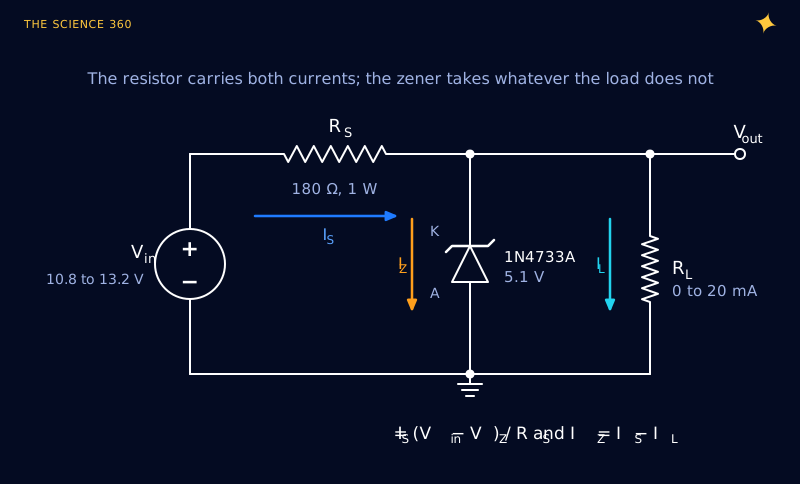
It is the same current-steering logic behind a resistor in series with an LED, with one twist: here a second branch, the load, competes for the current. It is also why a zener regulator behaves so differently from the plain voltage divider people try to use as a power supply. The divider's output sags in proportion to load; the zener branch gives up its own current first and holds the voltage until it runs out.
Which corner sets the resistor value?
Two things threaten regulation: too little zener current and too much. They happen at opposite corners of the operating range.
Too little zener current happens when the input is at its lowest, the load draws its maximum and the zener voltage is at the top of its tolerance (a higher VZ leaves less voltage across RS). That corner sets the largest resistor you can use. The onsemi "Zener Theory and Design Considerations" handbook writes it as:
Too much zener current happens at maximum input, minimum load (usually zero, because loads get unplugged) and the lowest zener voltage. That corner sets the zener's power rating:
Multiplying a current computed with VZ(min) by VZ(max) is slightly pessimistic, which is what you want from a worst case. This is also where page-one calculators go wrong most often: they compute the zener's power at your stated "typical" current, which is the one condition the zener is guaranteed never to stay in.
Worked example: 12 V to 5.1 V at up to 20 mA
The job: power a small sensor board that draws up to 20 mA at about 5 V from a 12 V adapter that can sit anywhere from 10.8 to 13.2 V (±10%). The load can be unplugged, so IL(min) = 0. The zener is the common 1N4733A, a 5.1 V, 1.3 W part in the Vishay DO-41 series. From its datasheet:
Ptot applies with leads 4 mm from the body held at ambient.
Step 1: choose the minimum zener current. The datasheet's 1 mA is a knee test point where the impedance can be 550 Ω, not a recommended operating current. I will set IZ(min) = 10 mA, which keeps the impedance down in the tens of ohms (Figure 2). More on that choice in the next section.
Step 2: size RS at the starved corner.
Nearest E12 value at or below: 180 Ω. Check:
Step 3: check the flooded corner.
The last line is the junction rise, with ideal lead cooling.
Well inside the 1.3 W rating. A 500 mW glass zener would also survive on paper, but at half its rating it would run hot and drift, which is a poor trade for a few cents.
Step 4: size the resistor's own power. This is the step most calculators skip, and the resistor is usually the hotter part:
Output shorted:
A 0.25 W resistor would cook. A 0.5 W part would run at 78% of its rating, which in a closed box is too close. Use a 1 W resistor, which also survives a shorted output indefinitely.
Step 5: tolerance sanity check. A 5% resistor may be 189 Ω. At the starved corner that gives , leaving 8.8 mA for the zener: a little under the 10 mA target but far from the knee. At 171 Ω and the flooded corner the zener takes 48.9 mA and 262 mW. Both are fine, which is the point of designing with margin.
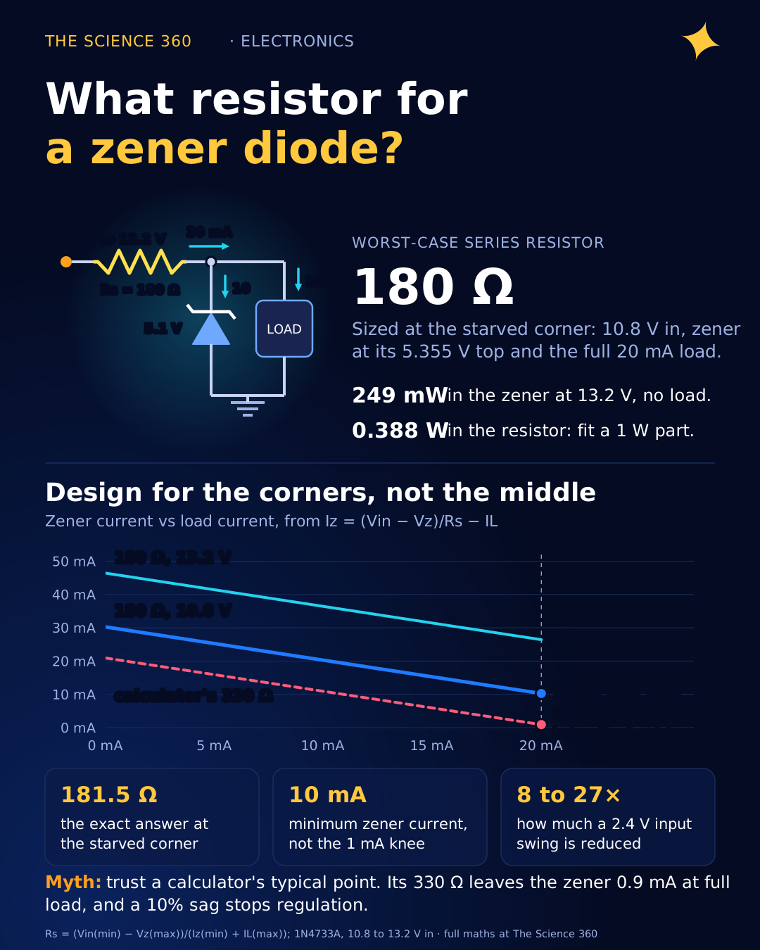
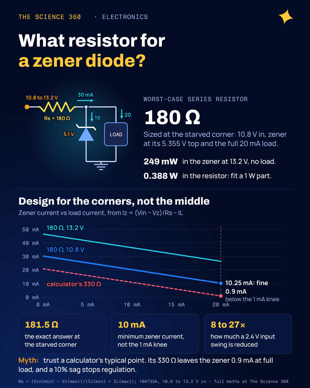
Figure 3 shows what the arithmetic means across the whole load range. Each line is , a straight line with slope −1. The design lives in the gap between the purple line (starved corner) and the green one (flooded corner). The dashed orange line is the calculator's 330 Ω answer, and you can see it cross into the knee right at the rated 20 mA load.
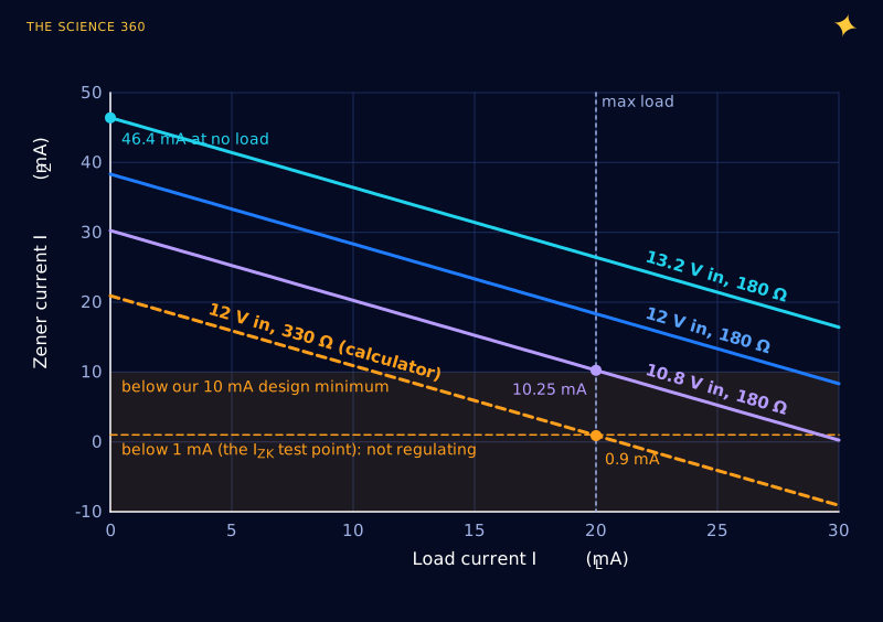
There is also a lower bound on RS. If you derate the 1N4733A to, say, half its rating (650 mW), the zener current must stay below , so . Anything from 69 to 181 Ω is a valid design; the high end wastes the least power.
What is the minimum zener current, really?
Zener datasheets list two currents, and neither is labeled "minimum operating current". The 1N4733A has IZT = 49 mA, the point where the 5.1 V ± 5% is guaranteed, and IZK = 1 mA, a point down in the knee where Vishay guarantees only that the impedance is below 550 Ω. onsemi's handbook describes IZT as usually at the quarter-power point and IZK as "an arbitrary low value in the knee region".
Why the impedance matters: the zener is not a perfect voltage source. Its slope in breakdown, , is its output resistance, and it falls steeply with current. The handbook notes that between IZK and IZT, impedance against current is close to a straight line on log-log axes, so the two datasheet points let you estimate the curve in between. Figure 2 does that for three Vishay parts.
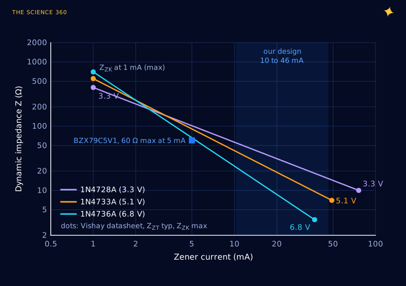
Plugging numbers into that interpolation for the 1N4733A gives roughly 90 Ω at 5 mA, 42 Ω at 10 mA, 19 Ω at 20 mA and 9 Ω at 40 mA. The 500 mW BZX79C5V1 from onsemi, specified at 5 mA, has a maximum of 60 Ω there, which lands on the same trend. So "10 mA minimum" for a 1 W part is not superstition: below that the zener is a soft spring rather than a stiff one.
There is a second, quieter consequence. The printed voltage is only promised at IZT. Integrate the impedance curve from 49 mA down to 10 mA and the 1N4733A's voltage could be around 0.6 V lower than at 49 mA. That is a large number, and probably pessimistic, because the curve mixes a typical value with a maximum one.
How well does a zener actually regulate?
Now that the design keeps the zener in breakdown, we can ask how much the output still moves. The onsemi handbook gives the full expression; for practical purposes it boils down to two small-signal rules (our simplification), with RZ the zener's dynamic impedance at the operating point:
Line regulation:
Load regulation:
Line regulation in our example. At full load, swinging the input from 10.8 to 13.2 V moves the zener current from about 11.7 to 25 mA. Using the datasheet's best-case 7 Ω gives the optimistic bound; the interpolated curve gives the pessimistic one:
Optimistic (RZ = 7 Ω):
Pessimistic (integrated curve, 11.7 to 25 mA):
So a 2.4 V swing on the input becomes somewhere between 0.09 and 0.3 V on the output: an improvement of 8 to 27 times, not the near-perfect clamp many tutorials imply. The same ratio applies to ripple. A 1 V peak-to-peak ripple from a rectifier and filter capacitor comes out at roughly 0.1 V peak-to-peak at full load with RZ near 20 Ω.
Load regulation. At 12 V in, going from no load to 20 mA moves the zener from 38.3 to 18.3 mA:
Optimistic:
Pessimistic (integrated curve, 38.3 to 18.3 mA):
Add temperature. The zener's own dissipation changes with load, so its junction temperature moves by up to about 27 K in this design. onsemi's BZX79C5V1 lists a temperature coefficient of −2.7 to +1.2 mV/K, which over 27 K is up to about 0.07 V. The 5.1 V region happens to be near the crossover between the zener mechanism (negative coefficient) and the avalanche mechanism (positive coefficient), which is why it is relatively stable thermally; the BZX79C6V8 is +1.2 to +4.5 mV/K.
Is a higher-voltage zener a better regulator?
Around 6 to 7 V, yes. The onsemi handbook says zeners below about 5 V break down by field emission with high impedance and a negative temperature coefficient, those above about 8 V by avalanche, and both mechanisms act in between. It notes that zeners around 7 V "will have remarkably low impedance". You can see it in Figure 2: the 6.8 V 1N4736A reaches 3.5 Ω where the 3.3 V 1N4728A is still at 10 Ω, and in the BZX79 series the 6.2 V part is specified at 10 Ω maximum against 95 Ω for the 3.3 V part, both at 5 mA. A low-voltage zener at a few milliamps is a poor regulator. If you need 3.3 V, think twice before reaching for a 3.3 V zener.
Why the zener runs hottest when nothing is connected
Figure 4 plots the power in each part at the flooded corner. The resistor's dissipation is a flat line: as long as the zener regulates, the voltage across RS is fixed, so its power is fixed. The zener's dissipation is a falling line that starts at its maximum with no load. The total power drawn from the supply never changes with load at all.
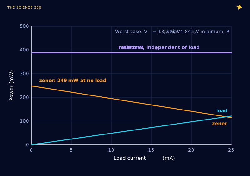
This is the least intuitive property of a shunt regulator and the root of most fried zeners. Someone builds the circuit, measures a comfortable zener temperature with the load running, then unplugs the load for the night. The zener now absorbs every milliamp the load was using.
It also explains the efficiency. At 12 V nominal and full load:
Efficiency is 0% at no load, with the same 0.46 W drawn.
The linear regulator heat problem is the same physics in a different package, except that a series regulator at least stops drawing current when the load does.
When a zener and resistor is the wrong tool
A zener shunt regulator earns its place as a reference, a clamp, or a supply for a few milliamps that rarely changes. It is a poor choice once the load is tens of milliamps and varies, for the reasons above. Three upgrades, in increasing order of effort:
Add an emitter follower. Put the zener on the base of an NPN transistor and take the output from the emitter. The zener now supplies only base current, roughly , so its current barely changes with load and RS can be much larger. The output sits one VBE (about 0.65 V) below VZ. Sizing that base drive is the same exercise as a transistor base resistor calculation, and the gain mechanism is covered in how a transistor amplifies.
Use a TL431 shunt reference. It drops into the same position as the zener but contains an amplifier. TI's datasheet gives a dynamic impedance of 0.2 Ω typical and 0.5 Ω maximum, and a minimum cathode current of 1 mA maximum. That is 35 times lower impedance than the 1N4733A's best-case 7 Ω, and it keeps regulating down to about a milliamp. Our 20 mA load step would move the output by about .
Use a real regulator. An LDO draws only what the load needs plus a small quiescent current. For larger drops or currents, a buck converter stops turning the difference into heat at all.
Whatever you pick, a 100 nF decoupling capacitor across the zener is cheap insurance. onsemi's handbook notes that zeners generate noise in the knee region, which falls off as current rises, and a capacitor shunts the high-frequency part to ground.
FAQ
How do you calculate the resistor for a zener diode?
Use the worst case: . Then check the opposite corner, maximum input with no load, for zener current and power. For 10.8 to 13.2 V in, a 1N4733A 5.1 V zener, 0 to 20 mA load and 10 mA minimum zener current, RS comes out at 181 Ω, so 180 Ω.
What is the minimum current for a zener diode?
There is no single number. Datasheets give a knee test current IZK, often 1 mA or 0.25 mA, where the impedance is still hundreds of ohms, and a test current IZT where the nominal voltage is guaranteed, 49 mA for a 1N4733A. A practical minimum is a few milliamps for small zeners and 5 to 10 mA or more for 1 W parts, and the voltage will sit below the printed value at low current.
When does a zener diode dissipate the most power?
With the load disconnected and the input at its maximum. In a shunt regulator the resistor current is fixed by the input voltage, so every milliamp the load stops drawing goes through the zener instead. Size the zener's power rating for that no-load case, not for normal operation.
Why does my zener give a lower voltage than its rating?
The rated voltage applies only at the datasheet test current, which is 49 mA for a 1N4733A 5.1 V zener. Run it at a few milliamps and it sits below 5.1 V, because the zener's dynamic impedance is high near the knee. Tolerance of ±5% and temperature add to the spread.
What wattage resistor do I need for a zener regulator?
The resistor dissipates whenever the zener is regulating, regardless of load. In the 12 V to 5.1 V example with 180 Ω that is 0.39 W at 13.2 V in, so use a 1 W part. If the output can be shorted, the resistor sees the full input: .
Related on The Science 360
Sources
- Vishay Semiconductors, 1N4728A to 1N4761A zener diodes datasheet, document 85816 rev. 2.7 (VZ, IZT, IZK, ZZT typical, ZZK maximum, ±5% tolerance, 1300 mW, RthJA 110 K/W): vishay.com/docs/85816/1n4728a.pdf
- onsemi, BZX79C2V4 to BZX79C18 zener diodes datasheet, rev. 5 (VZ range, ZZ maximum and temperature coefficient at 5 mA, 500 mW): onsemi.com BZX79C2V4/D
- onsemi, "TVS/Zener Theory and Design Considerations" handbook, HBD854/D (zener and avalanche mechanisms, impedance between IZK and IZT on log-log axes, low impedance near 7 V, knee noise, shunt regulator design equations 5 to 10): onsemi.com/pub/Collateral/HBD854-D.PDF
- Texas Instruments, TL431 / TL432 precision programmable reference datasheet (|ZKA| 0.2 Ω typical, 0.5 Ω maximum; Imin 1 mA maximum): ti.com/lit/ds/symlink/tl431.pdf
- Kunkune, Zener Diode Resistor Calculator (rounds the result down to the nearest E24 value): kunkune.co.uk zener calculator
- Calculate.co.nz, Zener Diode Resistor Calculator (typical single-point calculator: 12 V, 5 V, 20 mA example): calculate.co.nz/zener-diode-calculator.php
Method note: Figures 3 and 4 are direct evaluations of the shunt regulator equations with the datasheet tolerance limits. Figure 2 and the "pessimistic" regulation numbers use our own log-log interpolation between datasheet impedance points; they are estimates, not guaranteed values.
Header image: NASA (image jsc2025e015683), regraded for this article.