How wide should a PCB trace be?
On 1 oz outer copper with a 10 °C rise, IPC-2221 gives 11.8 mil (0.300 mm) for 1 A and 30.8 mil (0.781 mm) for 2 A. A 10 mil trace carries about 0.89 A. Inner layers need about 2.6 times the width for the same current.
The calculator uses the IPC-2221 curve fit; PCB trace width for current explains where it comes from and how the newer IPC-2152 data differs, and the companion post works through common signal and power widths.
Key results from the calculator
- 10 mil, 1 oz, outer: 0.89 A at 10 °C rise, 1.20 A at 20 °C; 0.44 A on an inner layer.
- 1 A: 11.8 mil outer, 30.8 mil inner (1 oz, 10 °C).
- 2 A: 30.8 mil outer, 80.0 mil inner.
- Doubling copper to 2 oz halves the width for the same current, because the formula works on cross-section area.
Six traces
Each example loads the current or width, copper weight, layer and temperature rise.
A 10 mil trace on 1 oz outer copper
Common default widthA 10 mil (0.254 mm) trace has 13.8 mil² of copper. At a 10 °C rise IPC-2221 allows 0.89 A; over 50 mm it measures 102.7 mΩ.
A 6 mil signal trace
Fine pitchA 6 mil (0.15 mm) trace is typical for fine-pitch signals. It still carries about 0.61 A on the surface at a 10 °C rise.
1 A on an outer layer
Small power rail11.8 mil (0.300 mm) on 1 oz copper keeps the rise to 10 °C. An inner layer would need 30.8 mil.
2 A on an inner layer
Buried traceIPC-2221 halves the allowed current for buried traces, so 2 A needs 80.0 mil inside against 30.8 mil on the surface. IPC-2152 data suggests that is conservative.
5 A on 2 oz outer copper
Motor or LED supplyThicker copper keeps it manageable: 54.4 mil (1.38 mm) on 2 oz. Over 100 mm it drops 94.3 mV.
10 A on 2 oz, 20 °C rise
High currentEven with a 20 °C allowance, 10 A needs 2.36 mm of 2 oz copper. Wide pours, planes or a bus bar are the usual answer.
Current for common widths (1 oz copper, IPC-2221)
| Width | mm | Outer, 10 °C | Outer, 20 °C | Inner, 10 °C |
|---|---|---|---|---|
| 6 mil | 0.152 mm | 0.61 A | 0.83 A | 0.31 A |
| 8 mil | 0.203 mm | 0.75 A | 1.02 A | 0.38 A |
| 10 mil | 0.254 mm | 0.89 A | 1.20 A | 0.44 A |
| 12 mil | 0.305 mm | 1.01 A | 1.37 A | 0.51 A |
| 16 mil | 0.406 mm | 1.25 A | 1.69 A | 0.62 A |
| 20 mil | 0.508 mm | 1.46 A | 1.99 A | 0.73 A |
| 30 mil | 0.762 mm | 1.96 A | 2.66 A | 0.98 A |
| 50 mil | 1.27 mm | 2.84 A | 3.86 A | 1.42 A |
| 100 mil | 2.54 mm | 4.70 A | 6.38 A | 2.35 A |
IPC-2221 curve fit with k = 0.048 (outer) and 0.024 (inner), 1 oz = 1.378 mil. The charts behind it cover up to 35 A, 400 mil, 10 to 100 °C rise and 0.5 to 3 oz copper.
How the calculator works
IPC-2221 curve fit: I = k × ΔT^0.44 × A^0.725, with A the copper cross-section in square mil and k = 0.048 for outer layers in air, 0.024 for inner layers. These constants come from fitting the IPC-2221 charts, as published with the Advanced Circuits calculator.
Width: cross-section divided by copper thickness, 1.378 mil (35 µm) per ounce per square foot.
Resistance: copper resistivity of 1/58 Ω·mm²/m at 20 °C, rising 0.393% per °C (NBS Handbook 100), at the ambient plus the allowed rise.
Drop and loss: V = I × R and P = I² × R over the length you enter.
What the model leaves out
- Nearby copper: planes and pours spread heat and let traces run cooler than IPC-2221 predicts; IPC-2152 accounts for this.
- Plating: outer layers get plated copper on top of the foil (about 20 µm on average by the IPC table NCAB describes), so a finished "1 oz" outer trace is often thicker than 35 µm.
- Board and enclosure: board thickness, airflow and a hot enclosure change the real temperature.
- Short pulses: a trace can carry more current for milliseconds than continuously.
Common misconceptions
"Inner traces are always hotter." IPC-2221 assumes so, but its internal chart was not based on tests; IPC-2152 testing found internal and external traces rise by about the same, and buried ones often run cooler.
"Width alone sets the current." Cross-section does: 2 oz copper doubles the area at the same width.
"The trace only needs to survive." A 10 °C rise is a comfortable design target; voltage drop on long power traces often matters first.
Frequently asked questions
How much current can a 10 mil trace carry?
About 0.89 A on 1 oz outer copper at a 10 °C rise, 1.20 A at 20 °C, and 0.44 A on an inner layer, by IPC-2221.
How wide should a trace be for 1 A?
11.8 mil (0.300 mm) on 1 oz outer copper for a 10 °C rise; 30.8 mil on an inner layer.
How thick is 1 oz copper?
1.378 mil, about 35 µm: one ounce of copper spread over a square foot.
Why do inner layers need wider traces?
IPC-2221 treats buried traces as insulated by the board, so it allows half the current. Newer IPC-2152 tests show this is often pessimistic.
Is IPC-2221 still valid?
It is a conservative rule of thumb that is still widely used. IPC-2152 replaced its charts with test data that accounts for board material and nearby planes.
Keep learning
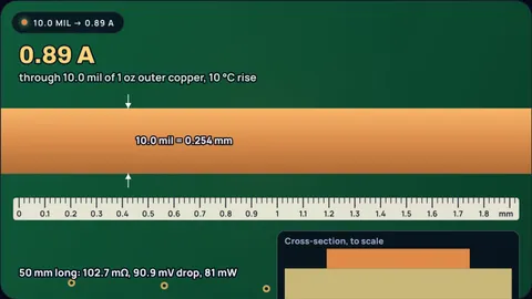
How Much Current Can a 10 mil Trace Carry? PCB Widths From 4 to 50 mil
A 10 mil trace on 1 oz outer copper carries about 0.89 A for a 10 °C rise and 1.2 A for 20 °C, by IPC-2221. A table for 4 to 50 mil, inner layers, 2 oz copper and the voltage drop.
PCB Trace Width for Current: IPC-2221 vs IPC-2152
IPC-2221 says internal traces need 2.6x the width. IPC-2152 test data says they run cooler. How to size a trace for 2 A, its voltage drop, and vias.
What Gauge Wire for 12V? Size for Voltage Drop
At 12 V, voltage drop, not ampacity, picks the wire. How to size 12 V wire from round-trip length and a 3% limit, with LED strip and fridge examples.