PCB Trace Width for Current: IPC-2221 vs IPC-2152
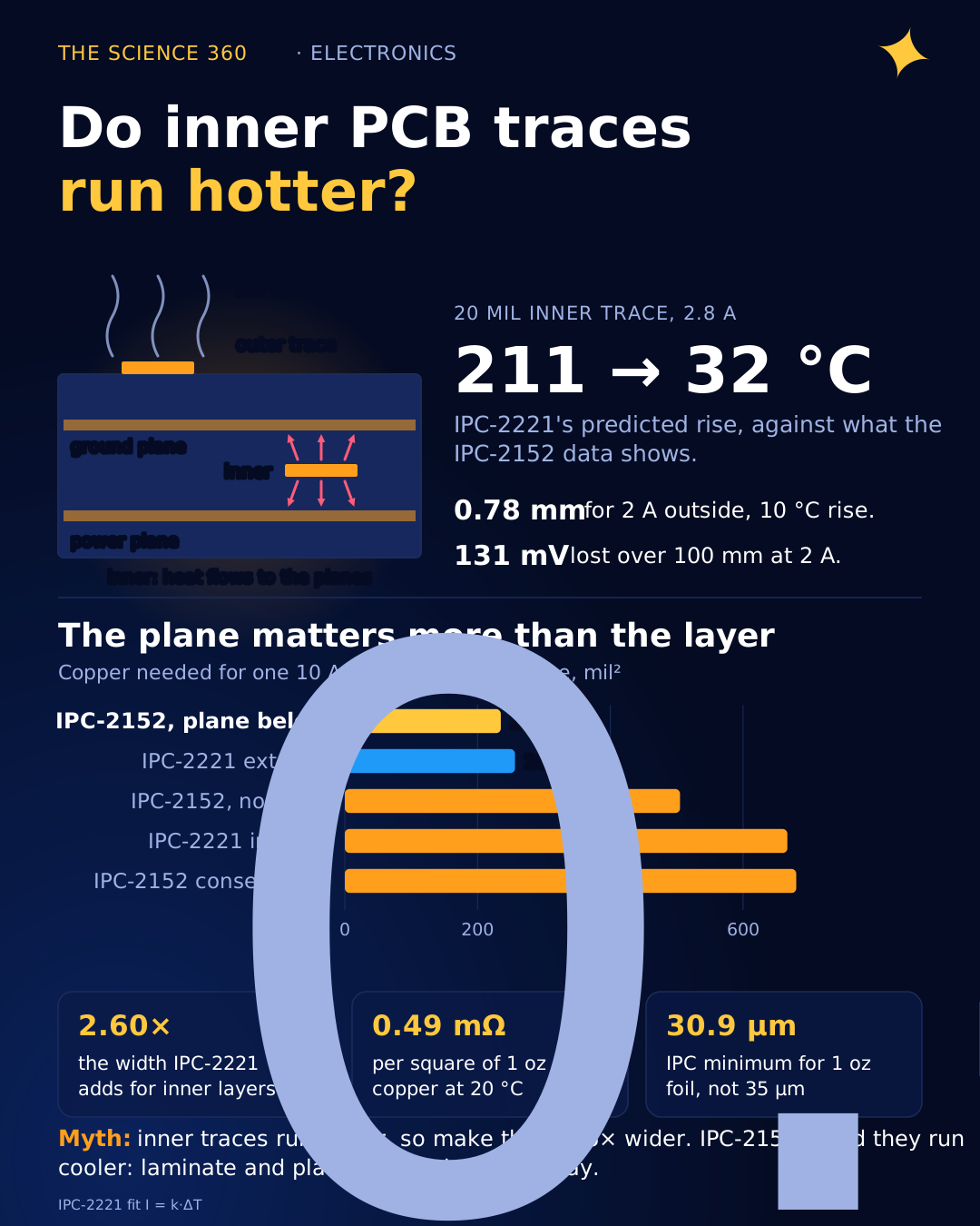
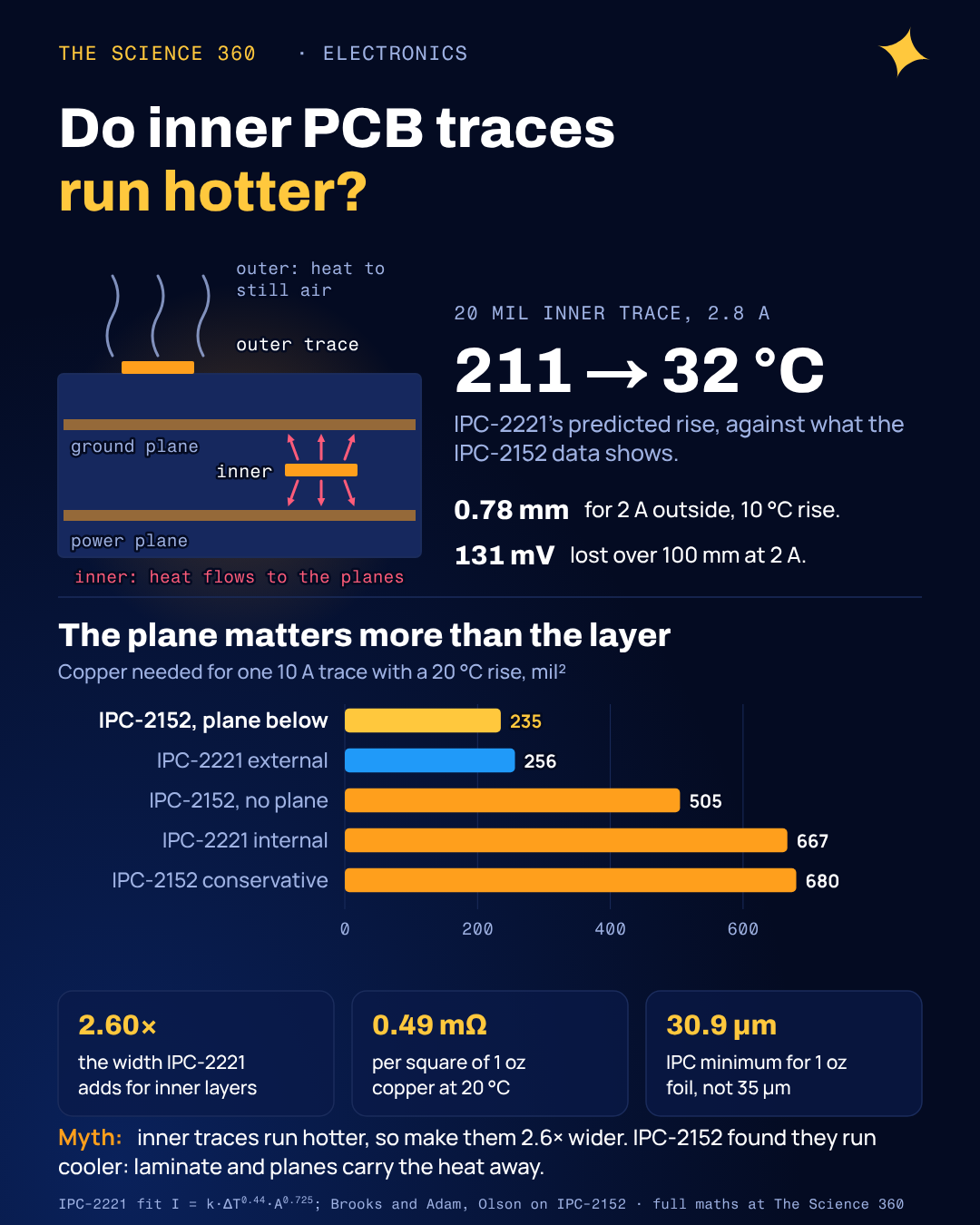
Take a 20 mil (0.51 mm) trace of 1 oz copper on an inner layer and push 2.8 A through it. The IPC-2221 formula that powers almost every online trace width calculator predicts a temperature rise of about 211 °C. Douglas Brooks and Johannes Adam, reading the measured data behind the newer IPC-2152 standard, put that same trace at about 32 °C above the board. Both numbers cannot be right, and the gap is not a rounding error. It is a misconception baked into a chart from the 1950s.
Page one for "pcb trace width for current" is mostly calculators. They are useful, and most of them faithfully implement IPC-2221, including its claim that internal traces need about two and a half times the width of external ones. This post shows where that formula comes from, what the newer data says about internal and external layers, and then does the calculation that matters for a real board: a 2 A trace on 1 oz copper, its voltage drop, and the vias that carry it between layers.
Where the IPC-2221 trace width formula comes from
The trace width charts in IPC-2221 go back to tests on surface traces in the 1950s. Jack Olson, in his tutorial on IPC-2152, describes the historical chart as "created over fifty years ago by the National Bureau of Standards", from a time with no multilayer boards. Calculators use a curve fit to those charts:
I = current (A), ΔT = temperature rise above ambient (°C), A = cross-section (square mils)
for external layers, 0.024 for internal layers
Width in mil, with the copper weight in oz:
Fit range: up to about 35 A, 400 mil wide, ΔT 10 to 100 °C, 0.5 to 3 oz copper
Those constants and limits are as given by Advanced Circuits' calculator, which says plainly that its formula "will simply extrapolate" outside the range of the original graphs. Rearranged for area:
Notice the exponent on A is 0.725, not 1. Doubling the copper cross-section gives you only times the current. A wide trace dissipates in proportion to its length, but sheds heat mostly from its surface, and the ratio gets worse as the trace widens. That is why there is no single "amps per millimetre" figure, a point most rules of thumb skip.
Worked example: how wide for 2 A on 1 oz copper?
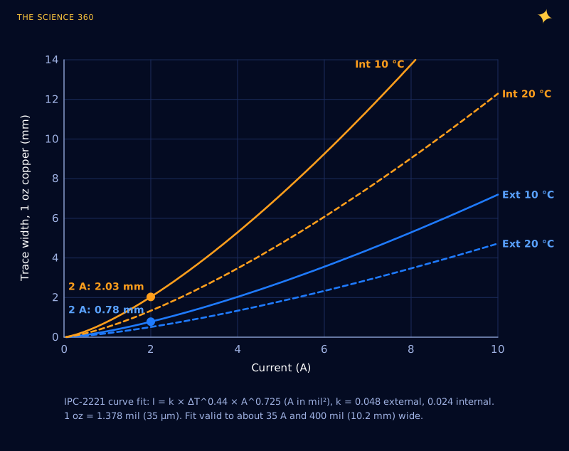
External layer, 10 °C rise
External, 20 °C rise:
Internal, 10 °C rise:
Internal, 20 °C rise:
The internal width is times the external one at any current, because halving k is all the formula does. Figure 1 shows the four curves from 0 to 10 A.
Are internal traces really hotter? What IPC-2152 found
Mike Jouppi, who led the testing that became IPC-2152 (published 2009), wrote that the historical internal chart "was not based on testing internal PCB conductors". It simply predicts half the current of the external chart for the same conductor. Olson's tutorial says the same thing more bluntly: "it is thought that when multi-layer board constructions became practical, the external values were merely doubled", and "this has since proven to be inaccurate."
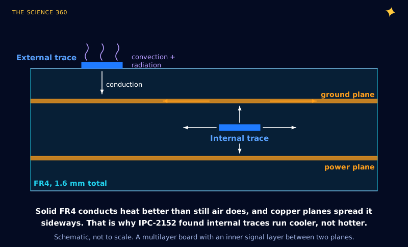
The physics was assumed backwards. An external trace loses heat to the air above it by convection and radiation, and into the board below by conduction. An internal trace is wrapped in laminate on all sides, and the old assumption was that being buried made it hotter. In fact, conduction through the dielectric, especially toward nearby copper planes, removes heat better than still air does. Olson: "in a still-air environment the internal traces actually run cooler than external." Brooks and Adam, working through 44 data points from IPC-2152, put it simply: "Internal traces are cooler everywhere."
How much cooler depends on the board. In Brooks and Adam's example, a 20 mil, 1 oz trace on a 60 mil FR4 board carrying 2.8 A rises 40 °C on the surface. At mid-board, the same trace rises . Compare that with the IPC-2221 fit:
Rearranged:
External:
IPC-2152: 40 °C, close.
Internal:
IPC-2152: 32 °C.
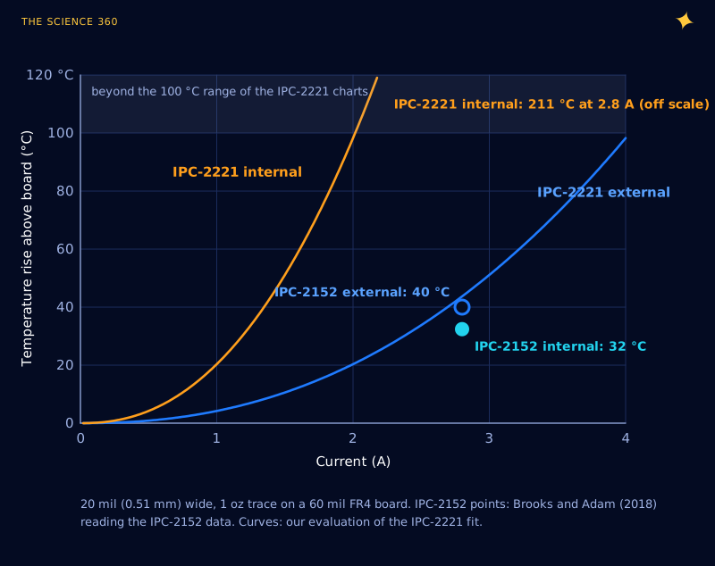
Why has nobody noticed? Because a rule that is too conservative never burns a board. Olson notes the internal values are "so conservative, however, that designers haven't experienced any problems using them except for the large amount of board real-estate needed." They simply cost you routing space, extra layers, or copper weight you did not need.
The catch: the external chart is not always safe either
The misconception cuts both ways. If you take away one thing from IPC-2152, it should not be "IPC-2221 is conservative, so go narrower." Olson reports that the new data "showed that the external trace chart was only safe for boards greater than 3x3in and with planes", which is why IPC-2152 dropped the historical external chart. A small two-layer board with no ground pour has nowhere to spread heat, and the external formula can underestimate its temperature.
The surprise in IPC-2152 is that the old internal chart survives, but with a new meaning. Olson: the internal values "by coincidence they very closely approximate the behavior of traces in free air", so IPC-2152 kept them as its "conservative chart", safe "in any circumstance except vacuum". In other words: use when you know nothing about the board, whatever layer the trace is on, and expect to be safe but wasteful.
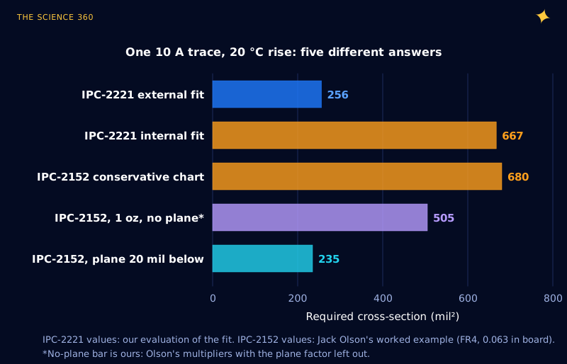
Olson's worked example shows the spread for one problem: a 10 A external trace with a 20 °C rise on a 0.063 in FR4 board 3 by 5 inches, with a 1 oz plane 20 mil below the surface layer. The answer depends almost entirely on what is under the trace.
Olson's IPC-2152 steps (10 A, 20 °C, external)
Universal chart value: 520 mil²
Conservative chart instead: 680 mil² → 530 mil wide
IPC-2221 external fit (our calculation): 256 mil² → 186 mil wide
Without the plane (our estimate):
So the old external formula happens to match the board with a plane, and would undersize the same trace on a board without one by about half. That is the honest summary: IPC-2221 is too pessimistic about inner layers and can be too optimistic about bare outer layers. The plane matters more than the layer.
What thickness is “1 oz” copper, really?
One ounce of copper spread over one square foot is 1.378 mil, or 35 µm, and every calculator divides by that. Your board may have less. Ruben Contreras of NCAB Group gives the IPC minimum for 1 oz foil as 30.9 µm (1.217 mil). Outer layers are often built from ½ oz foil plus plating, finishing at about 33.4 µm for Class 2 in his example. A trace that is 12% thinner than you assumed has 13% more resistance and runs hotter. If your design is marginal, ask the fabricator for the finished copper thickness rather than assuming 35 µm.
How much voltage does a PCB trace drop?
Temperature rise is only half the job. A trace is a resistor, and on long runs at low voltage the drop can matter more than the heat, exactly the trade-off in choosing wire gauge for 12 V. Copper's resistivity is 0.017241 Ω·mm²/m at 20 °C, rising by 0.393% per °C.
The 2 A, 0.78 mm external trace, 100 mm long
At 10 °C rise:
Drop and power at 2 A:
On a 3.3 V rail that is 4% of the supply, before the return path.
A handy shortcut is sheet resistance: 1 oz copper at 20 °C is per square. A trace 0.78 mm wide and 100 mm long is 128 squares, so 63 mΩ. If the load is a microcontroller core or a sensor reference, 131 mV matters, and the fix is a wider trace, a pour, or a remote-sense connection on the regulator. The ground return carries the same 2 A, so it drops the same again unless it is a solid plane. At switching frequencies, current crowds toward the trace surface and the edges, raising resistance further, which is the subject of skin effect and skin depth.
How much current can a via carry?
The via barrel is a short copper tube. Its cross-section is set by the drill size and the plating thickness, which fabricator sources put at an average of 20 µm for IPC Class 2 and 25 µm for Class 3 (per IPC-6012, which I have not read directly).
0.3 mm drill, 20 µm plating, 1.6 mm board
That is about a 0.5 mm wide 1 oz trace.
Treating it as an external trace at 10 °C:
For 2 A: use at least two vias; the drop through each is only about 1.6 to 3 mV.
Treating a via as a trace is a crude but common shortcut. A via is short and its ends are soldered to pads and pours that pull heat out of it, so in our view the estimate errs on the safe side. The resistance of a via is tiny; what usually limits it is the thin plating, not the length. Parallel vias also add redundancy if one has a plating void.
A trace width procedure that respects the board
1. Pick an allowed temperature rise from the local board temperature, not the room: hot parts nearby eat into it.
2. Start with IPC-2221 external () for surface traces over a plane, and with if you know nothing about the board or it has no planes.
3. Do not widen an internal trace just because it is internal; size it like an external one over a plane.
4. Use the real finished copper thickness.
5. Check voltage drop with , including the return path.
6. Size vias by barrel area, and use several in parallel for anything over about 1 A.
7. Parallel high-current traces heat each other: space them out or treat them as one wide trace.
For anything near its limits (motor drivers, power stages, battery leads), simulate it or measure it with a thermal camera on the first prototype. The trace that carries a stepper motor's coil current in an A4988 driver circuit or the switch node of a buck converter often sits next to a hot IC, and the copper under that IC doubles as its heatsink, which is a calculation of its own in heatsink thermal resistance. At the low-current end, the trace is rarely the limit: an Arduino pin's current limit runs out long before a 0.25 mm trace does.
FAQ
How wide should a PCB trace be for 1 A?
With the IPC-2221 formula on an external 1 oz layer, about 0.3 mm (12 mil) for a 10 °C rise and 0.2 mm (8 mil) for a 20 °C rise. Many designers use 0.5 mm per amp as a comfortable rule for short external runs, then check voltage drop on long ones.
How much current can a 1 oz trace carry per mm of width?
It is not linear, because wider traces shed heat less effectively per unit area. From the IPC-2221 fit for an external 1 oz trace and a 10 °C rise, 0.5 mm carries about 1.4 A, 1 mm about 2.4 A and 2 mm about 4 A.
Do internal traces need to be wider than external traces?
IPC-2221 says yes, by about 2.6 times for the same current. The newer IPC-2152, based on measurements, found internal traces run cooler than external ones of the same size, because the surrounding laminate conducts heat away better than air. The old internal chart is very conservative, not accurate.
How much current can a via carry?
A 0.3 mm via with 20 µm plating has a copper cross-section of about 0.018 mm², similar to a 0.5 mm wide 1 oz trace, and a resistance of about 1.6 mΩ through a 1.6 mm board. Treating it like a trace gives roughly 1 to 1.5 A. Use several vias in parallel for higher currents.
Related on The Science 360
Sources
- Jack Olson, "Determining Circuit Board Current Carrying Capability" (IPC-2152 tutorial: historical NBS chart, internal values doubled, conservative chart, external chart safe only above 3 by 3 in with planes, 10 A worked example): JackOlson-HowTo2152.pdf
- Michael Jouppi, "The New IPC-2152", Printed Circuit Design & Fab, July 2009 (internal chart not based on testing, half the external current): pcdandf.com
- Douglas Brooks and Johannes Adam, "Internal Trace Temperatures; More Complicated Than We Think", Signal Integrity Journal, 2020 (20 mil, 1 oz, 2.8 A, 40 °C external, 0.81 ratio mid-board): signalintegrityjournal.com
- Advanced Circuits, Trace Width Calculator (IPC-2221 fit: k = 0.048 and 0.024, exponents 0.44 and 0.725, 1.378 mil per oz, validity limits): advancedpcb.com trace width calculator
- Ruben Contreras, NCAB Group, "How Do You Calculate Finished Copper?", I-Connect007, 2020 (1 oz foil minimum 30.9 µm, plating averages 20 and 25 µm): iconnect007.com
- NBS Handbook 100, "Copper Wire Tables" (copper resistivity 0.017241 Ω·mm²/m and coefficient 0.00393 at 20 °C): nvlpubs.nist.gov
Method note: all IPC-2221 curves and widths are our evaluation of the published curve fit. IPC-2152 values are quoted from Olson and from Brooks and Adam; the no-plane estimate in Figure 4 and the via current estimate are our own.
Header image: NASA (image GRC-2006-C-01384), regraded for this article.